JAJSGG9B November 2018 – February 2024 TMUX1108
PRODUCTION DATA
- 1
- 1 特長
- 2 アプリケーション
- 3 概要
- 4 Device Comparison Table
- 5 Pin Configuration and Functions
-
6 Specifications
- 6.1 Absolute Maximum Ratings
- 6.2 ESD Ratings
- 6.3 Recommended Operating Conditions
- 6.4 Thermal Information
- 6.5 Electrical Characteristics (VDD = 5V ±10 %)
- 6.6 Electrical Characteristics (VDD = 3.3V ±10 %)
- 6.7 Electrical Characteristics (VDD = 2.5V ±10 %), (VSS = –2.5V ±10 %)
- 6.8 Electrical Characteristics (VDD = 1.8V ±10 %)
- 6.9 Electrical Characteristics (VDD = 1.2V ±10 %)
- 6.10 Typical Characteristics
- 7 Detailed Description
- 8 Application and Implementation
- 9 Device and Documentation Support
- 10Revision History
- 11Mechanical, Packaging, and Orderable Information
パッケージ・オプション
メカニカル・データ(パッケージ|ピン)
サーマルパッド・メカニカル・データ
発注情報
7.3.6 Ultra-low Charge Injection
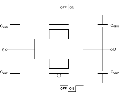
The TMUX1108 has a transmission gate topology, as shown in Figure 7-13. Any mismatch in the stray capacitance associated with the NMOS and PMOS causes an output level change whenever the switch is opened or closed.
 Figure 7-13 Transmission Gate Topology
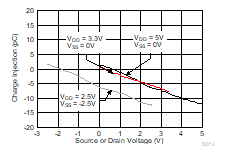
The TMUX1108 has special charge-injection cancellation circuitry that reduces the source-to-drain charge injection to as low as 1pC at VS = 1V as shown in Figure 7-14.
 Figure 7-14 Charge Injection vs Source or Drain Voltage