JAJSGS2C December 2018 – February 2024 TMUX1119
PRODUCTION DATA
- 1
- 1 特長
- 2 アプリケーション
- 3 概要
- 4 Pin Configuration and Functions
-
5 Specifications
- 5.1 Absolute Maximum Ratings
- 5.2 ESD Ratings
- 5.3 Recommended Operating Conditions
- 5.4 Thermal Information
- 5.5 Electrical Characteristics (VDD = 5V ±10 %)
- 5.6 Electrical Characteristics (VDD = 3.3V ±10 %)
- 5.7 Electrical Characteristics (VDD = 1.8V ±10 %)
- 5.8 Electrical Characteristics (VDD = 1.2V ±10 %)
- Typical Characteristics
- 6 Parameter Measurement Information
- 7 Detailed Description
- 8 Application and Implementation
- 9 Device and Documentation Support
- 10Revision History
- 11Mechanical, Packaging, and Orderable Information
パッケージ・オプション
メカニカル・データ(パッケージ|ピン)
サーマルパッド・メカニカル・データ
- DCK|6
発注情報
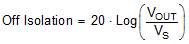
6.7 Off Isolation
Off isolation is defined as the ratio of the signal at the drain pin (D) of the device when a signal is applied to the source pin (Sx) of an off-channel. Figure 6-7 shows the setup used to measure, and the equation used to calculate off isolation.
 Figure 6-7 Off
Isolation Measurement Setup
Figure 6-7 Off
Isolation Measurement SetupEquation 2.