JAJSGS2C December 2018 – February 2024 TMUX1119
PRODUCTION DATA
- 1
- 1 特長
- 2 アプリケーション
- 3 概要
- 4 Pin Configuration and Functions
-
5 Specifications
- 5.1 Absolute Maximum Ratings
- 5.2 ESD Ratings
- 5.3 Recommended Operating Conditions
- 5.4 Thermal Information
- 5.5 Electrical Characteristics (VDD = 5V ±10 %)
- 5.6 Electrical Characteristics (VDD = 3.3V ±10 %)
- 5.7 Electrical Characteristics (VDD = 1.8V ±10 %)
- 5.8 Electrical Characteristics (VDD = 1.2V ±10 %)
- Typical Characteristics
- 6 Parameter Measurement Information
- 7 Detailed Description
- 8 Application and Implementation
- 9 Device and Documentation Support
- 10Revision History
- 11Mechanical, Packaging, and Orderable Information
パッケージ・オプション
メカニカル・データ(パッケージ|ピン)
サーマルパッド・メカニカル・データ
- DCK|6
発注情報
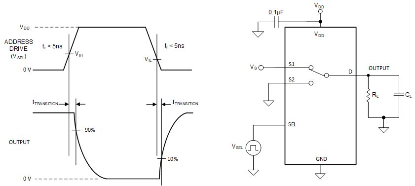
6.4 Transition Time
Transition time is defined as the time taken by the output of the device to rise or fall 10% after the address signal has risen or fallen past the logic threshold. The 10% transition measurement is utilized to provide the timing of the device. System level timing can then account for the time constant added from the load resistance and load capacitance. Figure 6-4 shows the setup used to measure transition time, denoted by the symbol tTRANSITION.
 Figure 6-4 Transition-Time Measurement Setup