JAJSHS9 August   2019 TMUX1247

PRODUCTION DATA.  

  1. 特長
  2. アプリケーション
  3. 概要
    1.     Device Images
      1.      アプリケーションの例
      2.      TMUX1247 のブロック図
  4. 改訂履歴
  5. Pin Configuration and Functions
    1.     Pin Functions
  6. Specifications
    1. 6.1 Absolute Maximum Ratings
    2. 6.2 ESD Ratings
    3. 6.3 Recommended Operating Conditions
    4. 6.4 Thermal Information
    5. 6.5 Electrical Characteristics (VDD = 5 V ±10 %), GND = 0 V unless otherwise specified.
    6. 6.6 Electrical Characteristics (VDD = 3.3 V ±10 %), GND = 0 V unless otherwise specified.
    7. 6.7 Electrical Characteristics (VDD = 1.8 V ±10 %), GND = 0 V unless otherwise specified.
    8. 6.8 Electrical Characteristics (VDD = 1.2 V ±10 %), GND = 0 V unless otherwise specified.
    9. 6.9 Typical Characteristics
  7. Parameter Measurement Information
    1. 7.1 On-Resistance
    2. 7.2 Off-Leakage Current
    3. 7.3 On-Leakage Current
    4. 7.4 Transition Time
    5. 7.5 Break-Before-Make
    6. 7.6 Charge Injection
    7. 7.7 Off Isolation
    8. 7.8 Crosstalk
    9. 7.9 Bandwidth
  8. Detailed Description
    1. 8.1 Overview
    2. 8.2 Functional Block Diagram
    3. 8.3 Feature Description
      1. 8.3.1 Bidirectional Operation
      2. 8.3.2 Rail to Rail Operation
      3. 8.3.3 1.8 V Logic Compatible Inputs
      4. 8.3.4 Fail-Safe Logic
    4. 8.4 Device Functional Modes
    5. 8.5 Truth Tables
  9. Application and Implementation
    1. 9.1 Application Information
    2. 9.2 Typical Application
      1. 9.2.1 Input Control for Power Amplifier
        1. 9.2.1.1 Design Requirements
        2. 9.2.1.2 Detailed Design Procedure
        3. 9.2.1.3 Application Curve
      2. 9.2.2 Switchable Operational Amplifier Gain Setting
        1. 9.2.2.1 Design Requirements
        2. 9.2.2.2 Detailed Design Procedure
        3. 9.2.2.3 Application Curve
  10. 10Power Supply Recommendations
  11. 11Layout
    1. 11.1 Layout Guidelines
      1. 11.1.1 Layout Information
    2. 11.2 Layout Example
  12. 12デバイスおよびドキュメントのサポート
    1. 12.1 ドキュメントのサポート
      1. 12.1.1 関連資料
    2. 12.2 ドキュメントの更新通知を受け取る方法
    3. 12.3 コミュニティ・リソース
    4. 12.4 商標
    5. 12.5 静電気放電に関する注意事項
    6. 12.6 Glossary
  13. 13メカニカル、パッケージ、および注文情報

パッケージ・オプション

メカニカル・データ(パッケージ|ピン)
サーマルパッド・メカニカル・データ
発注情報

Switchable Operational Amplifier Gain Setting

Another example application of the TMUX1247 is to change an Op Amp from unity gain setting to an inverting amplifier configuration. Utilizing a switch allows a system to have a configurable gain and allows the same architecture to be utilized across the board for various inputs to the system. Figure 19 shows the TMUX1247 configured for gain setting application.
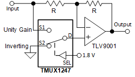
TMUX1247 1247-Gain.gifFigure 19. Switchable Op Amp Gain Setting