JAJSN29B october 2021 – march 2023 TMUX8211 , TMUX8212 , TMUX8213
PRODUCTION DATA
- 1 特長
- 2 アプリケーション
- 3 概要
- 4 Revision History
- 5 Device Comparison Table
- 6 Pin Configuration and Functions
-
7 Specifications
- 7.1 Absolute Maximum Ratings: TMUX821x Devices
- 7.2 ESD Ratings
- 7.3 Recommended Operating Conditions: TMUX821x Devices
- 7.4 ソースまたはドレイン連続電流
- 7.5 ドレイン・パルス電流のソース
- 7.6 Thermal Information
- 7.7 Electrical Characteristics (Global): TMUX821x Devices
- 7.8 Electrical Characteristics (±15-V Dual Supply)
- 7.9 Electrical Characteristics (±36-V Dual Supply)
- 7.10 Electrical Characteristics (±50-V Dual Supply)
- 7.11 Electrical Characteristics (72-V Single Supply)
- 7.12 Electrical Characteristics (100-V Single Supply)
- 7.13 Switching Characteristics: TMUX821x Devices
- 7.14 Typical Characteristics
- 8 Parameter Measurement Information
- 9 Detailed Description
- 10Application and Implementation
- 11Power Supply Recommendations
- 12Layout
- 13Device and Documentation Support
- 14Mechanical, Packaging, and Orderable Information
パッケージ・オプション
メカニカル・データ(パッケージ|ピン)
サーマルパッド・メカニカル・データ
- RUM|16
発注情報
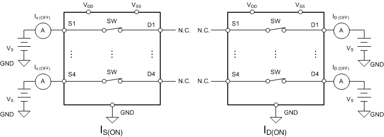
8.3 On-Leakage Current
Source On-Leakage current (IS(ON)) and drain On-Leakage current (ID(ON)) denote the channel leakage currents when the switch is in the on state. IS(ON) is measured with the drain floating, while ID(ON) is measured with the source floating. Figure 8-3 shows the circuit used for measuring the On-Leakage currents.
 Figure 8-3 On-Leakage Measurement Setup