JAJSHS8F June 2011 – February 2024 TPA6211A1-Q1
PRODUCTION DATA
- 1
- 1 特長
- 2 アプリケーション
- 3 概要
- 4 Pin Configuration and Functions
- 5 Specifications
- 6 Detailed Description
-
7 Application and Implementation
- 7.1 Application Information
- 7.2
Typical Applications
- 7.2.1
Typical Differential Input Application
- 7.2.1.1 Design Requirements
- 7.2.1.2 Detailed Design Procedure
- 7.2.1.3 Application Curves
- 7.2.2 Other Application Circuits
- 7.2.1
Typical Differential Input Application
- 8 Power Supply Recommendations
- 9 Layout
- 10Device and Documentation Support
- 11Revision History
- 12Mechanical, Packaging, and Orderable Information
パッケージ・オプション
メカニカル・データ(パッケージ|ピン)
- DGN|8
サーマルパッド・メカニカル・データ
- DGN|8
発注情報
6.3.3 Differential Output Versus Single-Ended Output
Figure 6-2 shows a Class-AB audio power amplifier (APA) in a fully differential configuration. The TPA6211A1-Q1 amplifier has differential outputs driving both ends of the load. One of several potential benefits to this configuration is power to the load. The differential drive to the speaker means that as one side is slewing up, the other side is slewing down, and vice versa. This in effect doubles the voltage swing on the load as compared to a ground-referenced load. Plugging 2 × VO(PP) into the power equation (Equation 14) yields four-times the output power (as the voltage is squared) from the same supply rail and load impedance (see Equation 16 and Equation 17).


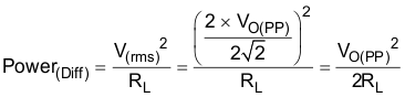

 Figure 6-2 Differential Output Configuration
In a typical automotive application operating at 5 V, bridging raises the power into an 8-Ω speaker from a singled-ended (SE, ground reference) limit of 390 mW to 1.56 W. This is a 6-dB improvement in sound power, or loudness of the sound. In addition to increased power, there are frequency-response concerns. Consider the single-supply SE configuration shown in Figure 6-3. A coupling capacitor (CC) is required to block the DC-offset voltage from the load. This capacitor can be quite large (approximately 33 µF to 1000 µF) so it tends to be expensive, heavy, occupy valuable PCB area, and have the additional drawback of limiting low-frequency performance. This frequency-limiting effect is due to the high-pass filter network created with the speaker impedance and the coupling capacitance. This is calculated with Equation 18.

For example, a 68-µF capacitor with an 8-Ω speaker would attenuate low frequencies below 293 Hz. The BTL configuration cancels the DC offsets, which eliminates the need for the blocking capacitors. Low-frequency performance is then limited only by the input network and speaker response. Cost and PCB space are also minimized by eliminating the bulky coupling capacitor.
 Figure 6-3 Single-Ended Output and Frequency Response
Increasing power to the load does carry a penalty of increased internal power dissipation. The increased dissipation is understandable considering that the BTL configuration produces four-times the output power of the SE configuration.