JAJSJN8C January 2016 – August 2020 TPD3S714-Q1
PRODUCTION DATA
- 1 特長
- 2 アプリケーション
- 3 概要
- 4 Revision History
- 5 Pin Configuration and Functions
- 6 Specifications
- 7 Parameter Measurement Information
-
8 Detailed Description
- 8.1 Overview
- 8.2 Functional Block Diagram
- 8.3
Feature Description
- 8.3.1 AEC-Q100 Qualified
- 8.3.2 Short-to-Battery and Short-to-Ground Protection on VBUS_CON
- 8.3.3 Short-to-Battery and Short-to-VBUS Protection on VD+, VD–
- 8.3.4 ESD Protection on VBUS_CON, VD+, VD–
- 8.3.5 Low RON nFET VBUS Switch
- 8.3.6 High Speed Data Switches
- 8.3.7 Hiccup Current Limit
- 8.3.8 Fast Overvoltage Response Time
- 8.3.9 Integrated Input Enable
- 8.3.10 Fault Output Signal
- 8.3.11 Thermal Shutdown Feature
- 8.3.12 16-pin SSOP Package
- 8.4 Device Functional Modes
- 9 Application and Implementation
- 10Power Supply Recommendations
- 11Layout
- 12Device and Documentation Support
- 13Mechanical, Packaging, and Orderable Information
9.2.3 Application Curves
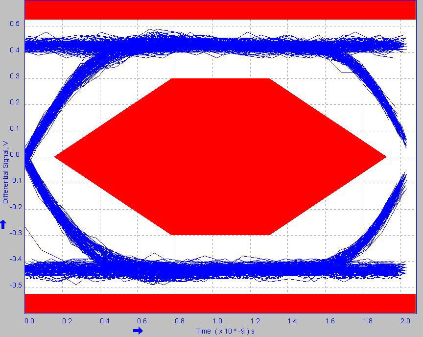
 Figure 9-2 USB2.0 Eye Diagram (Board Only, Through Path)
 Figure 9-4 50-V, 1-µF X7R Ceramic Shorted to 18-V (Not Recommended)
 Figure 9-6 TPD3S714-Q1 and 100-V, 1-µF X7R Shorted to 18 V (Powered Off)
 Figure 9-3 USB2.0 Eye Diagram (System from Typical Application Schematic)
 Figure 9-5 100-V, 1-µF X7R Ceramic Shorted to 18 V