JAJSRJ3D December   2012  – October 2023 TPD4E1B06

PRODUCTION DATA  

  1.   1
  2. 特長
  3. アプリケーション
  4. 概要
  5. Revision History
  6. Pin Configuration and Functions
  7. Specifications
    1. 6.1 Absolute Maximum Ratings
    2. 6.2 ESD Ratings
    3. 6.3 Recommended Operating Conditions
    4. 6.4 Thermal Information
    5. 6.5 Electrical Characteristics
    6. 6.6 Typical Characteristics
  8. Detailed Description
    1. 7.1 Overview
    2. 7.2 Functional Block Diagram
    3. 7.3 Feature Description
      1. 7.3.1 Ultra Low Leakage Current 0.5 nA (Maximum)
      2. 7.3.2 Transient Protection for 4 I/O Lines
      3. 7.3.3 I/O Capacitance 0.7 pF (Typical)
      4. 7.3.4 Bi-Directional (ESD) Protection Diode Array
      5. 7.3.5 Low ESD Clamping Voltage
    4. 7.4 Device Functional Modes
  9. Application and Implementation
    1. 8.1 Application Information
    2. 8.2 Typical Application
      1. 8.2.1 Design Requirements
      2. 8.2.2 Detailed Design Procedure
        1. 8.2.2.1 Signal Range on IO1, IO2, IO3, and IO4 Pins
        2. 8.2.2.2 Operating Frequency
      3. 8.2.3 Application Curves
    3. 8.3 Layout
      1. 8.3.1 Layout Guidelines
      2. 8.3.2 Layout Examples
  10. Device and Documentation Support
    1. 9.1 ドキュメントの更新通知を受け取る方法
    2. 9.2 サポート・リソース
    3. 9.3 Trademarks
    4. 9.4 静電気放電に関する注意事項
    5. 9.5 用語集
  11. 10Mechanical, Packaging, and Orderable Information

パッケージ・オプション

メカニカル・データ(パッケージ|ピン)
サーマルパッド・メカニカル・データ
発注情報

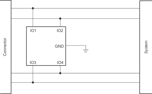
Typical Application

GUID-1DDB571B-4936-4AFF-8F64-489DA29C1B89-low.gifFigure 8-1 Protecting a Pair of Bi-Directional Differential Data Lines

The typical application of the TBD4E1B06 is to be placed in between the connector and the system. The low capacitance of the TBD4E1B06 gives flexibility in the end application, as it can be used on many different high speed interfaces.