SNAS629C JULY   2013  – December 2014 TPL5100

PRODUCTION DATA.  

  1. Features
  2. Applications
  3. Description
  4. Revision History
  5. Pin Configuration and Functions
  6. Specifications
    1. 6.1 Absolute Maximum Ratings
    2. 6.2 ESD Ratings
    3. 6.3 Recommended Operating Ratings
    4. 6.4 Thermal Information
    5. 6.5 Electrical Characteristics
    6. 6.6 Timing Requirements TCAL, MOS_DRV, DONE, PGOOD
    7. 6.7 Typical Characteristics
  7. Detailed Description
    1. 7.1 Overview
    2. 7.2 Functional Block Diagram
    3. 7.3 Feature Description
      1. 7.3.1 Supervisor Feature
      2. 7.3.2 Calibration Pulse
        1. 7.3.2.1 Overview of the Timing Signals MOS_DRV, TCAL, and DONE
      3. 7.3.3 Configuration and Interface
    4. 7.4 Device Functional Modes
  8. Application and Implementation
    1. 8.1 Application Information
    2. 8.2 Typical Application
      1. 8.2.1 Design Requirements
      2. 8.2.2 Detailed Design Procedure
      3. 8.2.3 Application Curve
  9. Power Supply Recommendations
  10. 10Layout
    1. 10.1 Layout Guidelines
    2. 10.2 Layout Example
  11. 11Device and Documentation Support
    1. 11.1 Trademarks
    2. 11.2 Electrostatic Discharge Caution
    3. 11.3 Glossary
  12. 12Mechanical, Packaging, and Orderable Information

パッケージ・オプション

メカニカル・データ(パッケージ|ピン)
サーマルパッド・メカニカル・データ
発注情報

10 Layout

10.1 Layout Guidelines

The more sensitive pins of the TPL5100 are the digital input pins D0, D1, D2 to select the timer interval. It is mandatory to connect them to VDD or GND through short traces avoiding series resistance. Moreover, it is mandatory to keep these pins far from traces of high frequency signals, such as clock or communication bus. Signal integrity of DRV and TCAL signal is achieved reducing parasitic capacitance on the traces between the TPL5100 and the microcontroller.

10.2 Layout Example

LAYOUT2.gif
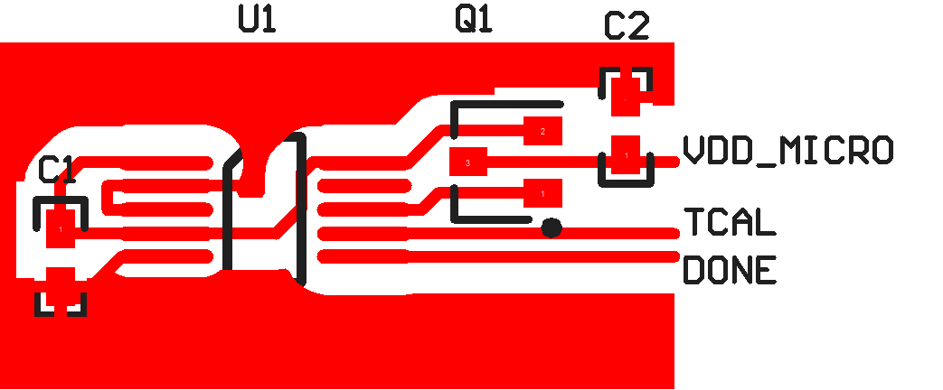
Figure 9. Board Layout