JAJSM93B june 2022 – may 2023 TPS1641
PRODUCTION DATA
- 1
- 1 特長
- 2 アプリケーション
- 3 概要
- 4 Revision History
- 5 Device Comparison Table
- 6 Pin Configuration and Functions
- 7 Specifications
-
8 Detailed Description
- 8.1 Overview
- 8.2 Functional Block Diagram
- 8.3
Feature Description
- 8.3.1 Enable and Shutdown Input (EN/SHDN)
- 8.3.2 Overvoltage Protection (OVP)
- 8.3.3 Output Slew Rate and Inrush Current Control (dVdt)
- 8.3.4 Active Current Limiting (ILIM) With the TPS16412, TPS16413, TPS16416, and TPS16417
- 8.3.5 Active Power Limiting (PLIM) With the TPS16410, TPS16411, TPS16414, and TPS16415
- 8.3.6 Overcurrent Protection (IOCP) and Blanking Time (IDLY or PDLY) for Transient Loads
- 8.3.7 Fast-Trip and Short-Circuit Protection
- 8.3.8 Analog Load Current Monitor (IMON) on the IOCP Pin
- 8.3.9 IN to OUT Short Detection (TPS16410, TPS16411, TPS16412, and TPS16413)
- 8.3.10 Thermal Shutdown and Overtemperature Protection
- 8.3.11 Fault Response and Indication (FLT)
- 8.4 Device Functional Modes
- 9 Application and Implementation
- 10Device and Documentation Support
- 11Mechanical, Packaging, and Orderable Information
パッケージ・オプション
メカニカル・データ(パッケージ|ピン)
- DRC|10
サーマルパッド・メカニカル・データ
- DRC|10
発注情報
8.3.7 Fast-Trip and Short-Circuit Protection
During an output short-circuit event, the current through the device increases very rapidly. When an output short-circuit is detected and output current reaches ISCP level, the device turns off the internal FET after a delay of tSCP_dly.
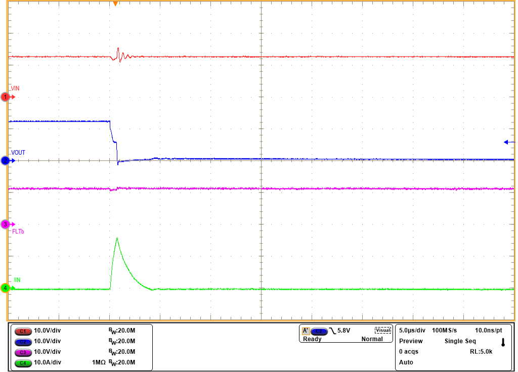
In case of fast input transients, the current through internal FET rises rapidly, but these transients can lead to false turn-off of internal FET due to excessive flow of current through internal FET. To prevent false tripping during these input transients, the device includes fast-trip comparator, which turns off the internal FET if the output current exceeds Ifast-trip for a duration of tfast-trip. Figure 8-14 shows the short-circuit response of the device.
 Figure 8-14 Short-Circuit Response with
VIN = 12 V