SLVSB49F November 2011 – January 2015 TPS22910A , TPS22912C
PRODUCTION DATA.
- 1 Features
- 2 Applications
- 3 Description
- 4 Simplified Schematic
- 5 Revision History
- 6 Device Comparison Table
- 7 Pin Configuration and Functions
-
8 Specifications
- 8.1 Absolute Maximum Ratings
- 8.2 ESD Ratings
- 8.3 Recommended Operating Conditions
- 8.4 Thermal Information
- 8.5 Electrical Characteristics
- 8.6 Switching Characteristics, Typical
- 8.7 Typical DC Characteristics
- 8.8 Typical AC Characteristics, TPS22910A
- 8.9 Typical AC Characteristics, TPS22912C
- 8.10 Typical AC Characteristics, TPS22913B
- 8.11 Typical AC Characteristics, TPS22913C
- 9 Parameter Measurement Information
- 10Detailed Description
- 11Application and Implementation
- 12Power Supply Recommendations
- 13Layout
- 14Device and Documentation Support
- 15Mechanical, Packaging, and Orderable Information
11 Application and Implementation
11.1 Application Information
This section will highlight some of the design considerations when implementing this device in various applications. A PSPICE model for this device is also available in the product page of this device on www.ti.com for further aid.
11.1.1 VIN to VOUT Voltage Drop
The VIN to VOUT voltage drop in the device is determined by the RON of the device and the load current. The RON of the device depends upon the VIN condition of the device. Refer to the RON specification of the device in the Electrical Characteristics table of this datasheet. Once the RON of the device is determined based upon the VIN conditions, use Equation 1 to calculate the VIN to VOUT voltage drop:
Where,
ΔV = Voltage drop from VIN to VOUT
ILOAD = Load current
RON = On-resistance of the device for a specific VIN
An appropriate ILOAD must be chosen such that the IMAX specification of the device is not violated.
11.1.2 On/Off Control
The ON pin controls the state of the switch. The ON pin has a low threshold, making it capable of interfacing with low-voltage signals. The ON pin is compatible with standard GPIO logic thresholds. It can be used with any microcontroller with 1.2 V or higher GPIO voltage. This pin cannot be left floating and must be driven either high or low for proper functionality.
11.1.3 Input Capacitor (Optional)
To limit the voltage drop on the input supply caused by transient inrush currents when the switch turns on into a discharged load capacitor or short-circuit, a capacitor needs to be placed between VIN and GND. A 1-µF ceramic capacitor, CIN, placed close to the pins, is usually sufficient. Higher values of CIN can be used to further reduce the voltage drop during high current applications. When switching heavy loads, it is recommended to have an input capacitor about 10 times higher than the output capacitor to avoid excessive voltage drop.
11.1.4 Output Capacitor (Optional)
Due to the integrated body diode in the PMOS switch, a CIN greater than CL is highly recommended. A CL greater than CIN can cause VOUT to exceed VIN when the system supply is removed. This could result in current flow through the body diode from VOUT to VIN. A CIN to CL ratio of 10 to 1 is recommended for minimizing VIN dip caused by inrush currents during startup, however a 10 to 1 ratio for capacitance is not required for proper functionality of the device. A ratio smaller than 10 to 1 (such as 1 to 1) could cause slightly more VIN dip upon turn-on due to inrush currents. This can be mitigated by using a device with a longer rise time.
11.2 Typical Application
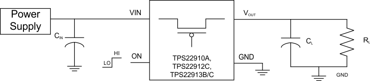 Figure 50. Typical Application
11.2.1 Design Requirements
| Design Parameter | Example Value |
|---|---|
| VIN | 1.5 V to 5 V |
| CL | 0.1 µF to 1 µF |
| Maximum Acceptable Inrush Current | 1 A |
11.2.2 Detailed Design Procedure
11.2.2.1 Inrush Current
When the switch is enabled, the output capacitors must be charged up from 0-V to VIN voltage. This charge arrives in the form of inrush current. Inrush current can be calculated using the following equation:
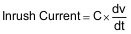
Where,
C = Output capacitance
 = Output slew rate
The TPS22910A, TPS22912C, and TPS22913B/C offer several different rise time options to control the inrush current during turn-on. The appropriate device can be selected based upon the maximum acceptable slew rate which can be calculated using the design requirements and the inrush current equation. An output capacitance of 1.0 µF will be used since the inrush follows the following equations:
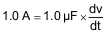

To ensure an inrush current of less than 1 A, a device with a slew rate less than 1 V/µs must be used
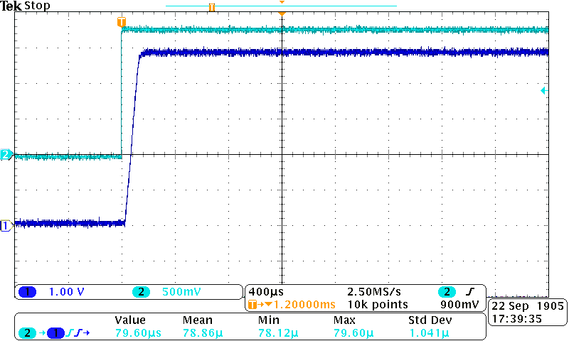
The TPS22910A has a typical rise time of 1 µs at 3.3 V . This results in a slew rate of 3.3 V/µs which is above the 1 V/µs requirement meaning the TPS22910 could not be used to meet the design requirements.
The TPS22913B has a typical rise time of 66 µs at 3.3 V. This results in a slew rate of 50 mV/µs which is below the 1 V/µs requirement; therefor, the TPS22913B could be used to meet the design requirements. The TPS22912C or TPS22913C have lower slew rates than the TPS22913B, so they could also be used, but the output would rise more slowly.
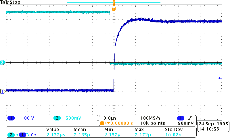
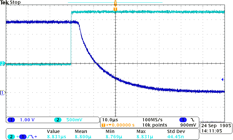
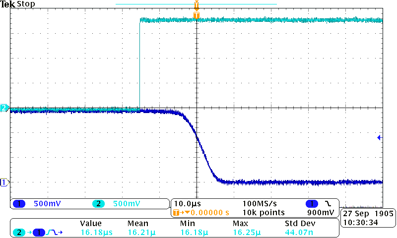
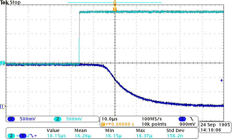
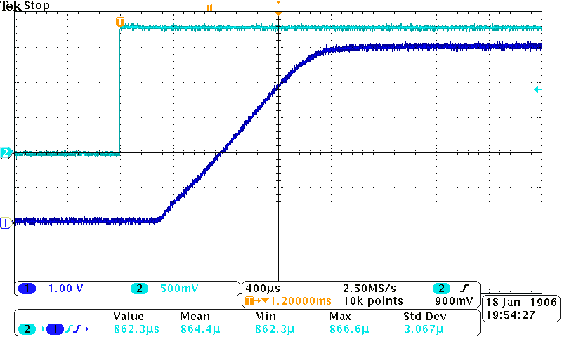
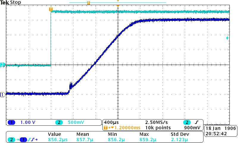
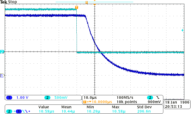
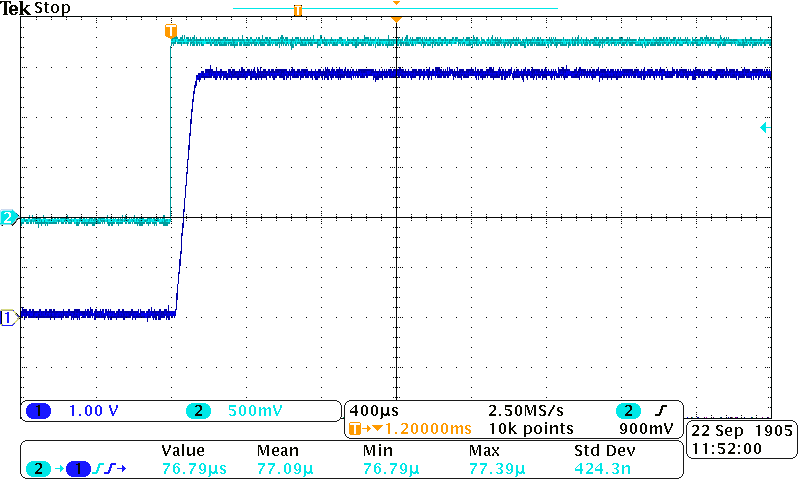
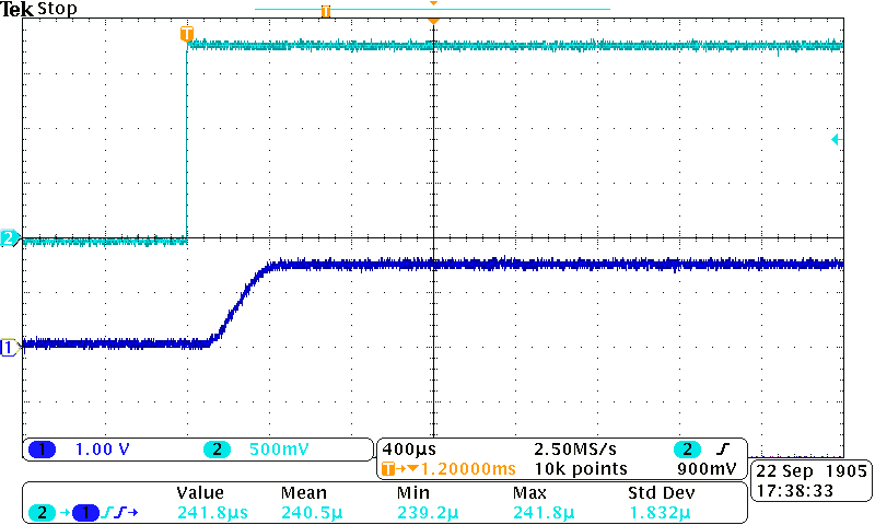
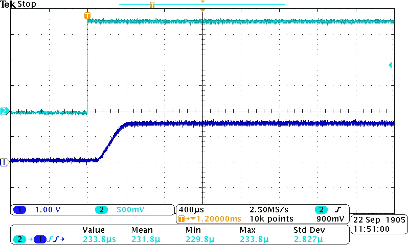
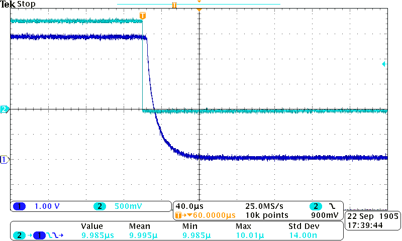
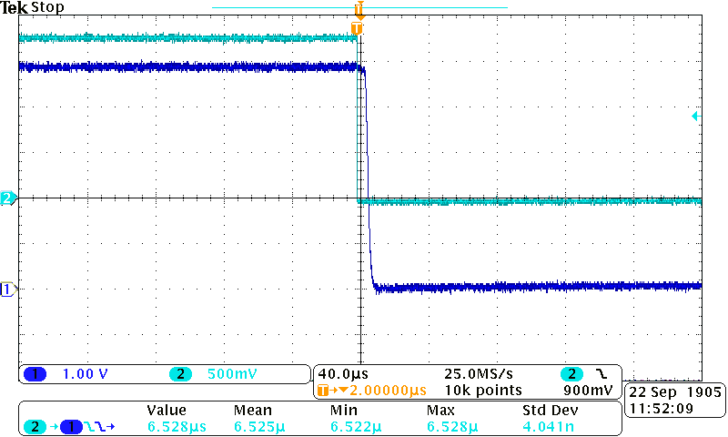
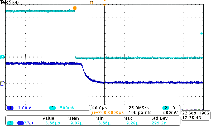
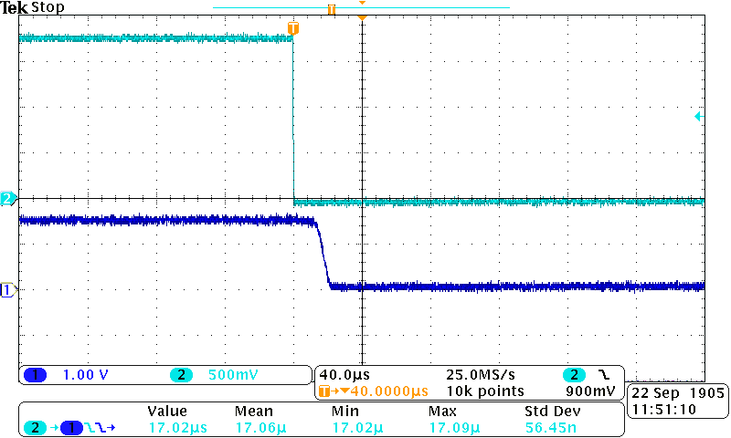
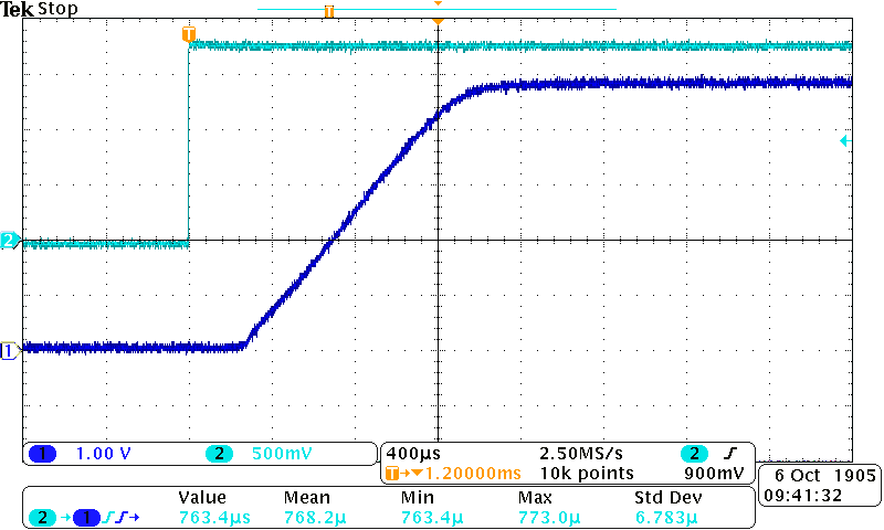
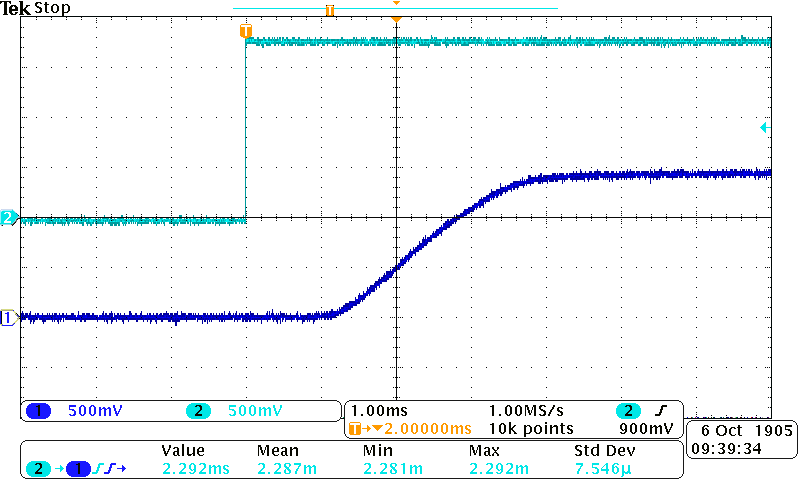
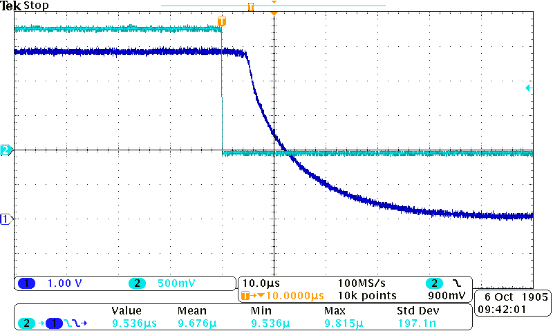
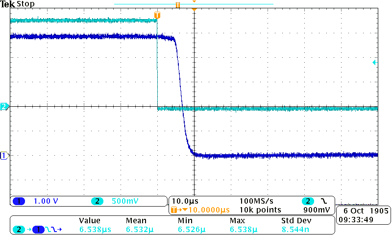
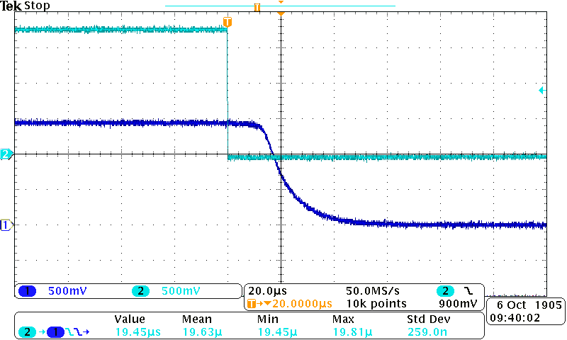
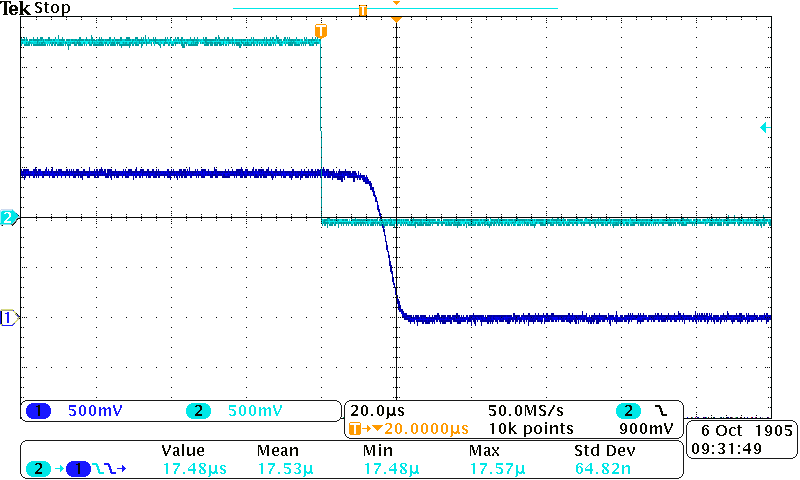
11.2.3 Application Curves
11.2.3.1 Typical Application Characteristics for TPS22910A
The dark blue curve (Channel 1) represents the VOUT pin of the device. The light blue curve (Channel 2) represents the ON pin of the device.
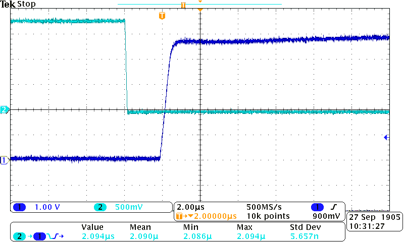
| VIN = 5 V | TA = 25°C | CIN = 10 µF |
| CL = 0.1 µF | RL = 10Ω |
| VIN = 5 V | TA = 25°C | CIN =10 µF |
| CL = 1 µF | RL = 10 Ω |
| VIN = 1.5 V | TA = 25°C | CIN = 10 µF |
| CL = 0.1 µF | RL = 10Ω |
| VIN = 1.5 V | TA = 25°C | CIN = 10 µF |
| CL = 1 µF | RL = 10Ω | |
| VIN = 5 V | TA = 25°C | CIN = 10 µF |
| CL = 0.1 µF | RL = 10Ω |
| VIN = 5 V | TA = 25°C | CIN = 10 µF |
| CL = 1 µF | RL = 10Ω |
| VIN = 1.5 V | TA = 25°C | CIN = 10 µF |
| CL = 0.1 µF | RL = 10Ω |
| VIN = 1.5 V | TA = 25°C | CIN = 10 µF |
| CL = 1 µF | RL = 10Ω |
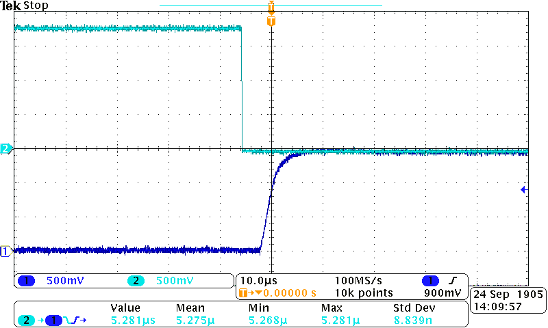
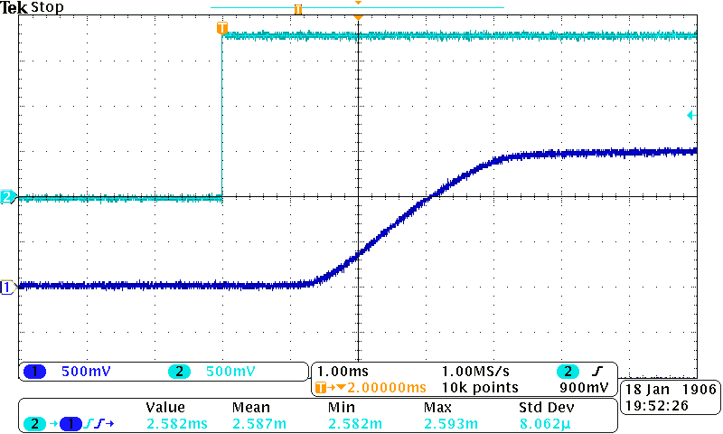
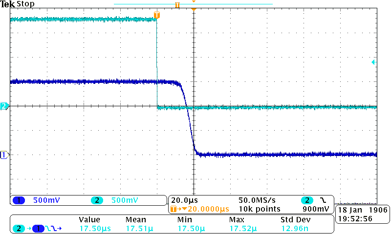
11.2.3.2 Typical Application Characteristics for TPS22912C
The dark blue curve (Channel 1) represents the VOUT pin of the device. The light blue curve (Channel 2) represents the ON pin of the device.
| VIN = 5 V | TA = 25°C | CIN = 1 µF |
| CL = 0.1 µF | RL = 10Ω |
| VIN = 5 V | TA = 25°C | CIN =10 µF |
| CL = 1 µF | RL = 10 Ω |
| VIN = 1.5 V | TA = 25°C | CIN = 1 µF |
| CL = 0.1 µF | RL = 10 Ω |
| VIN = 1.5 V | TA = 25°C | CIN = 10 µF |
| CL = 1 µF | RL = 10 Ω |
| VIN = 5 V | TA = 25°C | CIN = 1 µF |
| CL = 0.1 µF | RL = 10 Ω |
| VIN = 5 | TA = 25°C | CIN = 10 µF |
| CL = 1 µF | RL = 10 Ω |
| VIN = 1.5 V | TA = 25°C | CIN = 1 µF |
| CL = 0.1 µF | RL = 10 Ω |
| VIN = 1.5 V | TA = 25°C | CIN = 10 µF |
| CL = 1 µF | RL = 10 Ω |
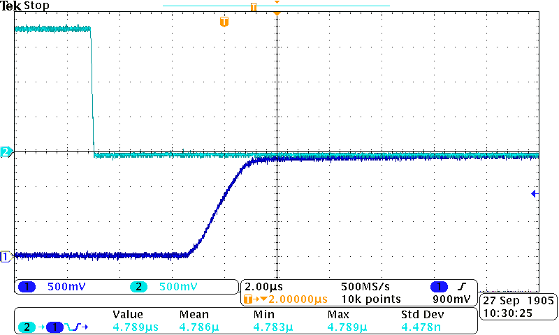
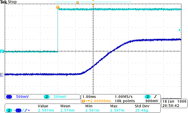
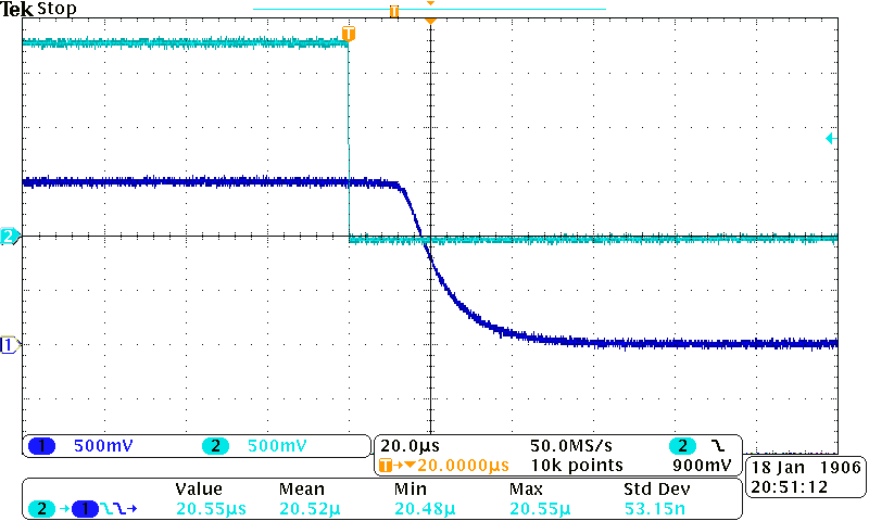
11.2.3.3 Typical Application Characteristics For TPS22913B
The dark blue curve (Channel 1) represents the VOUT pin of the device. The light blue curve (Channel 2) represents the ON pin of the device.
| VIN = 5 V | TA = 25°C | CIN = 10 µF |
| CL = 1 µF | RL = 10 Ω |
| VIN = 5 V | TA = 25°C | CIN = 1 µF |
| CL = 0.1 µF | RL = 10 Ω |
| VIN = 1.5 V | TA = 25°C | CIN = 10 µF |
| CL = 1 µF | RL = 10 Ω |
| VIN = 1.5 V | TA = 25°C | CIN = 1 µF |
| CL = 0.1 µF | RL = 10 Ω |
| VIN = 5 V | TA = 25°C | CIN = 10 µF |
| CL = 1 µF | RL = 10 Ω |
| VIN = 5 V | TA = 25°C | CIN = 1 µF |
| CL = 0.1 µF | RL = 10 Ω |
| VIN = 1.5 V | TA = 25°C | CIN = 10 µF |
| CL = 1 µF | RL = 10 Ω |
| VIN = 1.5 V | TA = 25°C | CIN = 1 µF |
| CL = 0.1 µF | RL = 10 Ω |
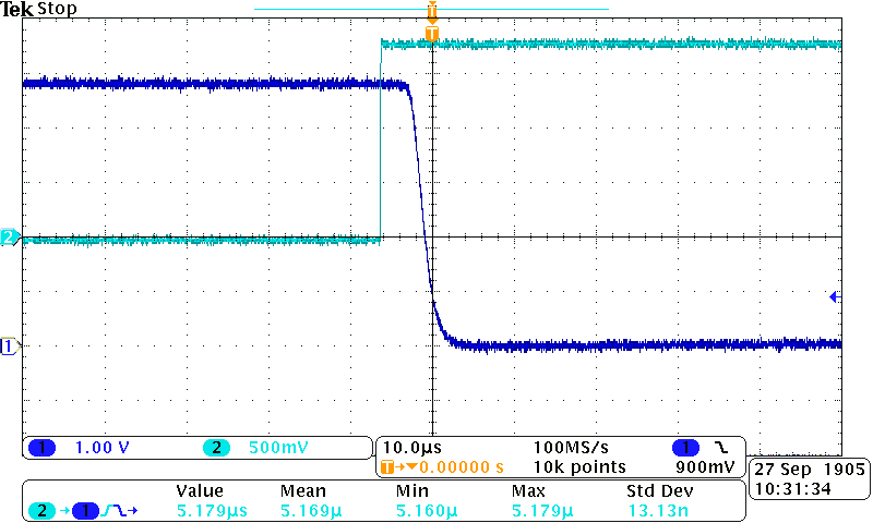
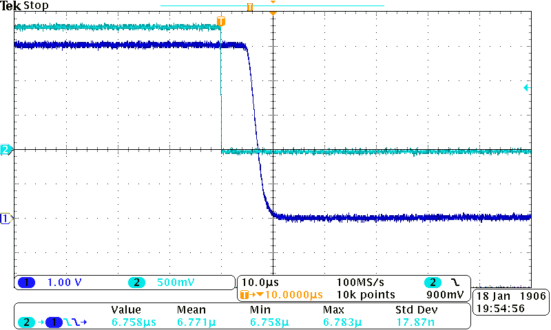
11.2.3.4 Typical Application Characteristics for TPS22913C
The dark blue curve (Channel 1) represents the VOUT pin of the device. The light blue curve (Channel 2) represents the ON pin of the device.
| VIN = 5 V | TA = 25°C | CIN = 10 µF |
| CL = 1 µF | RL = 10 Ω |

| VIN = 5 V | TA = 25°C | CIN = 1 µF |
| CL = 0.1 µF | RL = 10 Ω |
| VIN = 1.5 V | TA = 25°C | CIN = 10 µF |
| CL = 1 µF | RL = 10 Ω |

| VIN = 1.5 V | TA = 25°C | CIN = 1 µF |
| CL = 0.1 µF | RL = 10 Ω |
| VIN = 5 V | TA = 25°C | CIN = 10 µF |
| CL = 1 µF | RL = 10 Ω |
| VIN = 5 V | TA = 25°C | CIN = 1 µF |
| CL = 0.1 µF | RL = 10 Ω |
| VIN = 1.5 V | TA = 25°C | CIN = 10 µF |
| CL = 1 µF | RL = 10 Ω |
| VIN = 1.5 V | TA = 25°C | CIN = 1 µF |
| CL = 0.1 µF | RL = 10 Ω |