SLVSB49F November 2011 – January 2015 TPS22910A , TPS22912C
PRODUCTION DATA.
- 1 Features
- 2 Applications
- 3 Description
- 4 Simplified Schematic
- 5 Revision History
- 6 Device Comparison Table
- 7 Pin Configuration and Functions
-
8 Specifications
- 8.1 Absolute Maximum Ratings
- 8.2 ESD Ratings
- 8.3 Recommended Operating Conditions
- 8.4 Thermal Information
- 8.5 Electrical Characteristics
- 8.6 Switching Characteristics, Typical
- 8.7 Typical DC Characteristics
- 8.8 Typical AC Characteristics, TPS22910A
- 8.9 Typical AC Characteristics, TPS22912C
- 8.10 Typical AC Characteristics, TPS22913B
- 8.11 Typical AC Characteristics, TPS22913C
- 9 Parameter Measurement Information
- 10Detailed Description
- 11Application and Implementation
- 12Power Supply Recommendations
- 13Layout
- 14Device and Documentation Support
- 15Mechanical, Packaging, and Orderable Information
8 Specifications
8.1 Absolute Maximum Ratings
| MIN | MAX | UNIT | |||
|---|---|---|---|---|---|
| VIN | Input voltage range | –0.3 | 6 | V | |
| VOUT | Output voltage range | –0.3 | 6 | V | |
| VON | Input voltage range | –0.3 | 6 | V | |
| IMAX | Maximum continuous switch current | 2 | A | ||
| IPLS | Maximum pulsed switch current, pulse < 300 µs, 2% duty cycle | 2.5 | A | ||
| TA | Operating free-air temperature range | –40 | 85 | °C | |
| TJ | Maximum junction temperature | 125 | °C | ||
| Tstg | Storage temperature range | –65 | 150 | °C | |
8.2 ESD Ratings
| VALUE | UNIT | |||
|---|---|---|---|---|
| V(ESD) | Electrostatic discharge | Human-body model (HBM), per ANSI/ESDA/JEDEC JS-001(1) | ±2000 | V |
| Charged-device model (CDM), per JEDEC specification JESD22-C101(2) | ±1000 | |||
(1) JEDEC document JEP155 states that 500-V HBM allows safe manufacturing with a standard ESD control process. Manufacturing with less than 500-V HBM is possible with the necessary precautions. Pins listed as ±2000 V may actually have higher performance.
(2) JEDEC document JEP157 states that 250-V CDM allows safe manufacturing with a standard ESD control process. Manufacturing with less than 250-V CDM is possible with the necessary precautions. Pins listed as ±1000 V may actually have higher performance.
8.3 Recommended Operating Conditions
| MIN | MAX | UNIT | |||
|---|---|---|---|---|---|
| VIN | Input voltage range | 1.4 | 5.5 | V | |
| VON | ON voltage range | 0 | 5.5 | V | |
| VOUT | Output voltage range | VIN | |||
| VIH | High-level input voltage, ON | VIN = 1.4 V to 5.5 V | 1.1 | 5.5 | V |
| VIL | Low-level input voltage, ON | VIN = 3.61 V to 5.5 V | 0.6 | V | |
| VIN = 1.4 V to 3.6 V | 0.4 | V | |||
| CIN | Input capacitor | 1(1) | µF | ||
(1) Refer to the application section.
8.4 Thermal Information
| THERMAL METRIC(1) | TPS22910 | TPS22912 | TPS22913 | UNIT | |
|---|---|---|---|---|---|
| CSP | CSP | CSP | |||
| 4 PINS | 4 PINS | 4 PINS | |||
| RθJA | Junction-to-ambient thermal resistance | 189.1 | 189.1 | 189.1 | °C/W |
| RθJCtop | Junction-to-case (top) thermal resistance | 1.9 | 1.9 | 1.9 | |
| RθJB | Junction-to-board thermal resistance | 36.8 | 36.8 | 36.8 | |
| ψJT | Junction-to-top characterization parameter | 11.3 | 11.3 | 11.3 | |
| ψJB | Junction-to-board characterization parameter | 36.8 | 36.8 | 36.8 | |
(1) For more information about traditional and new thermal metrics, see the IC Package Thermal Metrics application report, SPRA953.
8.5 Electrical Characteristics
The electrical characteristics in this section apply to all devices unless otherwise noted. For TPS22910A VON = 0 V where enabled and VON = VIN where disabled. For TPS22912C and TPS22913B/C VON = VIN where enabled and VON = 0 V where disabled. VIN = 1.4 V to 5.5 V, TA = –40ºC to 85ºC (unless otherwise noted)| PARAMETER | TEST CONDITIONS | TA | MIN | TYP | MAX | UNIT | |
|---|---|---|---|---|---|---|---|
| IIN | Quiescent current | IOUT = 0 mA, VIN = 5.25 V, VON = Enabled | Full | 2 | 10 | µA | |
| IOUT = 0 mA, VIN = 4.2 V, VON = Enabled | 2 | 7.0 | |||||
| IOUT = 0 mA, VIN = 3.6 V, VON = Enabled | 2 | 7.0 | |||||
| IOUT = 0 mA, VIN = 2.5 V, VON = Enabled | 0.9 | 5 | |||||
| IOUT = 0 mA, VIN = 1.5 V, VON = Enabled | 0.7 | 5 | |||||
| IIN(off) | Off supply current | RL = 1 MΩ, VIN = 5.25 V, VON = Disabled | Full | 1.2 | 10 | µA | |
| RL = 1 MΩ, VIN = 4.2 V, VON = Disabled | 0.2 | 7.0 | |||||
| RL = 1 MΩ, VIN= 3.6 V, VON = Disabled | 0.1 | 7.0 | |||||
| RL = 1 MΩ, VIN = 2.5 V, VON = Disabled | 0.1 | 5 | |||||
| RL = 1 MΩ, VIN = 1.5 V, VON = Disabled | 0.1 | 5 | |||||
| IIN(Leakage) | Leakage current | VOUT = 0 V, VIN= 5.25 V, VON = Disabled | Full | 1.2 | 10 | µA | |
| VOUT = 0 V, VIN = 4.2 V, VON = Disabled | 0.2 | 7.0 | |||||
| VOUT = 0 V, VIN = 3.6 V, VON = Disabled | 0.1 | 7.0 | |||||
| VOUT = 0 V, VIN = 2.5 V, VON = Disabled | 0.1 | 5 | |||||
| VOUT = 0 V, VIN = 1.5 V, VON = Disabled | 0.1 | 5 | |||||
| rON | On-resistance | VIN = 5.25 V, IOUT = –200 mA | 25°C | 60 | 80 | mΩ | |
| Full | 110 | ||||||
| VIN = 5.0 V, IOUT = –200 mA | 25°C | 60 | 80 | ||||
| Full | 110 | ||||||
| VIN = 4.2 V, IOUT = –200 mA | 25°C | 60 | 80 | ||||
| Full | 110 | ||||||
| VIN = 3.3 V, IOUT = –200 mA | 25°C | 60.7 | 80 | ||||
| Full | 110 | ||||||
| VIN = 2.5 V, IOUT = –200 mA | 25°C | 63.4 | 90 | ||||
| Full | 120 | ||||||
| VIN = 1.8 V, IOUT = –200 mA | 25°C | 74.2 | 100 | ||||
| Full | 130 | ||||||
| VIN = 1.5 V, IOUT = –200 mA | 25°C | 83.9 | 120 | ||||
| Full | 150 | ||||||
| RPD(1) | Output pull down resistance | VIN = 3.3 V, IOUT = 30 mA, VON = 0 | 25°C | 153 | 200 | Ω | |
| UVLO | Under voltage lockout | VIN increasing, VON = 0 V, IOUT = –100 mA |
Full | 1.2 | V | ||
| VIN decreasing, VON = 0 V, RL = 10 Ω | 0.50 | ||||||
| ION | ON input leakage current | VON = 1.4 V to 5.25 V or GND | Full | 1 | µA | ||
| VRCP | Reverse current voltage threshold | TPS22910A, TPS22913B/C | 44 | mV | |||
| TPS22912C | 54 | ||||||
| tDELAY | Reverse current response delay | VIN = 5 V | 10 | µs | |||
| IRCP(leak) | Reverse current protection leakage after reverse current event. | VOUT – VIN > VRCP | 25°C | 0.3 | µA | ||
(1) Only applies to the TPS22913B/C devices
8.6 Switching Characteristics, Typical
| PARAMETER | TEST CONDITION | TPS22910A | TPS22912C | TPS22913B | TPS22913C | UNIT | |
|---|---|---|---|---|---|---|---|
| VIN = 5 V, TA = 25ºC (unless otherwise noted) | |||||||
| tON | Turn-ON time | RL = 10 Ω, CL = 0.1 µF | 2 | 840 | 76 | 770 | µs |
| tOFF | Turn-OFF time | RL = 10 Ω, CL = 0.1 µF | 5.5 | 6.6 | 6.6 | 6.6 | |
| tR | VOUT rise time | RL = 10 Ω, CL = 0.1 µF | 1 | 912 | 82 | 838 | |
| tF | VOUT fall time | RL = 10 Ω, CL = 0.1 µF | 3 | 3 | 3 | 3 | |
| VIN = 3.3 V, TA = 25ºC (unless otherwise noted) | |||||||
| tON | Turn-ON time | RL = 10 Ω, CL = 0.1 µF | 2.5 | 1147 | 102 | 1048 | µs |
| tOFF | Turn-OFF time | RL = 10 Ω, CL = 0.1 µF | 7 | 8.6 | 8.5 | 8.6 | |
| tR | VOUT rise time | RL = 10 Ω, CL = 0.1 µF | 1 | 1030 | 97 | 980 | |
| tF | VOUT fall time | RL = 10 Ω, CL = 0.1 µF | 3.5 | 3 | 3 | 3 | |
| VIN = 1.5 V, TA = 25ºC (unless otherwise noted) | |||||||
| tON | Turn-ON time | RL = 10 Ω, CL = 0.1 µF | 4.5 | 2513 | 234 | 2344 | µs |
| tOFF | Turn-OFF time | RL = 10 Ω, CL = 0.1 µF | 16.5 | 17.4 | 17 | 18 | |
| tR | VOUT rise time | RL = 10 Ω, CL = 0.1 µF | 2 | 1970 | 244 | 1823 | |
| tF | VOUT fall time | RL = 10 Ω, CL = 0.1 µF | 7 | 6.5 | 6.5 | 6.5 | |
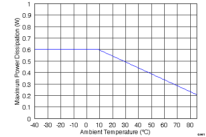
8.7 Typical DC Characteristics
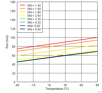
The typical characteristics curves in this section apply to all devices unless otherwise noted.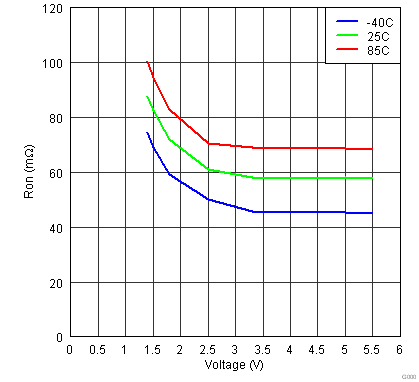 Figure 1. On-State Resistance vs Input Voltage
 Figure 3. TPS22912C and TPS22913B/C On Input Threshold (Active High)
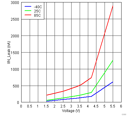
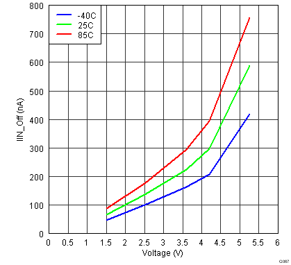 Figure 7. Input Current, Off vs Input Voltage
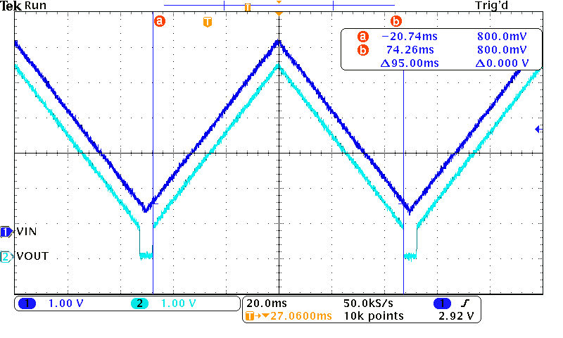 Figure 9. Under Voltage Lockout Response
(IOUT = –100mA)
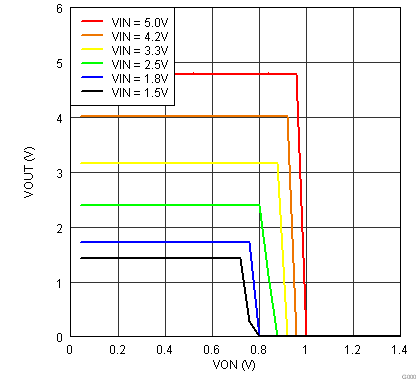 Figure 2. TPS22910A On Input Threshold (Active Low)
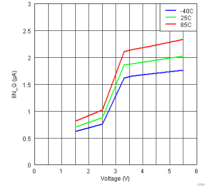 Figure 4. Input Current, Quiescent vs Input Voltage
|
|
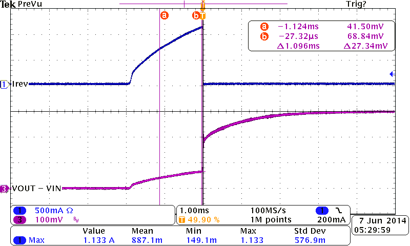 Figure 10. Full-Time Reverse Current Protection
(VIN = 3.0 V, VOUT Ramp up From 3.0 V to 3.3 V)
8.8 Typical AC Characteristics, TPS22910A
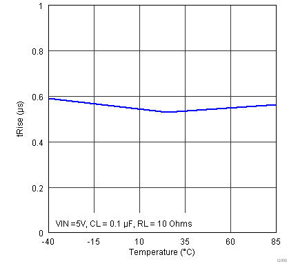
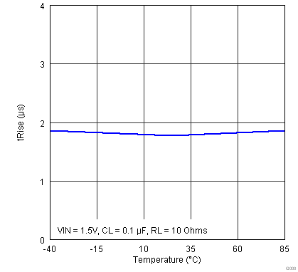
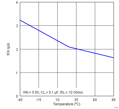
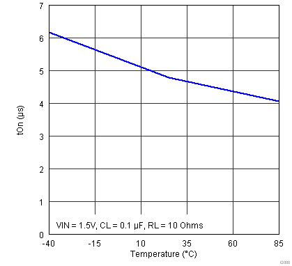 Figure 17. Turn-on Time vs Temperature
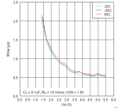 Figure 19. Rise Time vs Input Voltage
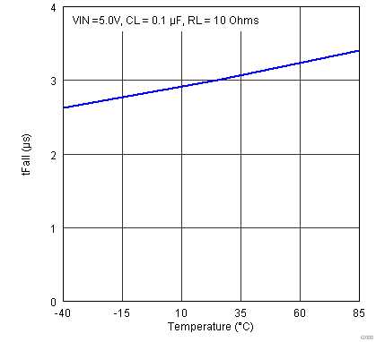
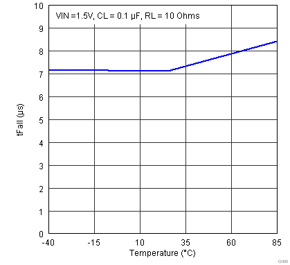
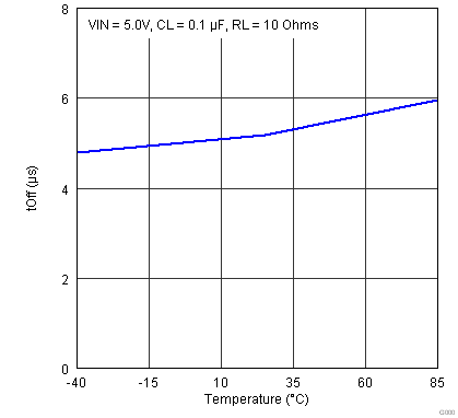
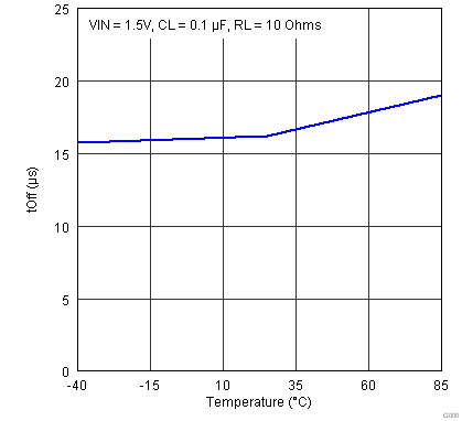 Figure 18. Turn-off Time vs Temperature
8.9 Typical AC Characteristics, TPS22912C
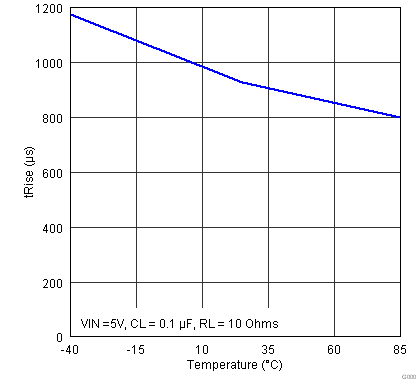
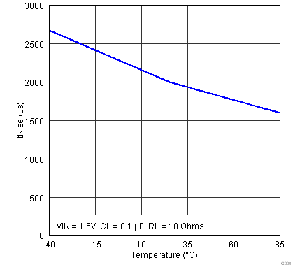
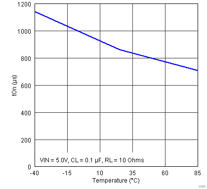
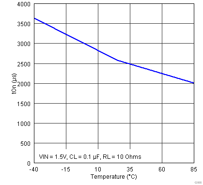 Figure 26. Turn-on Time vs Temperature
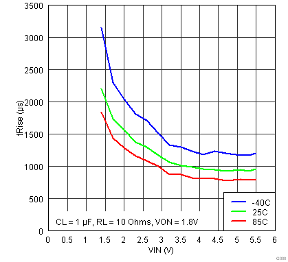 Figure 28. Rise Time vs Input Voltage
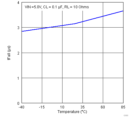
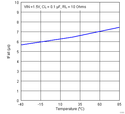
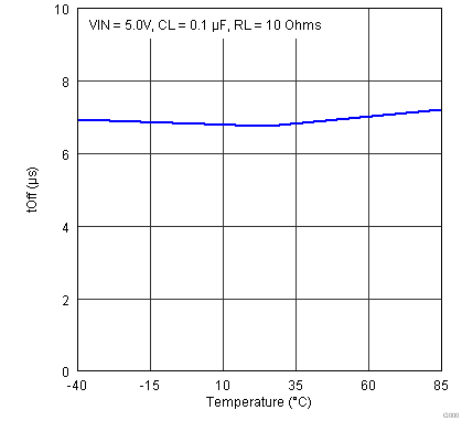
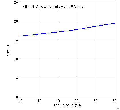 Figure 27. Turn-off Time vs Temperature
8.10 Typical AC Characteristics, TPS22913B
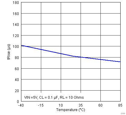
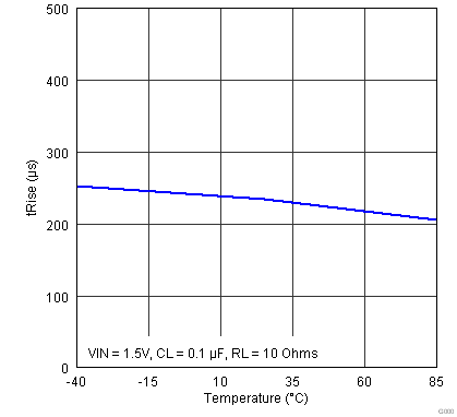
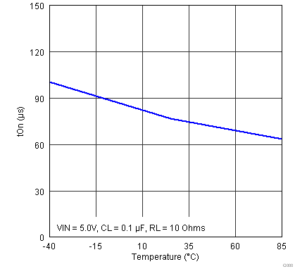
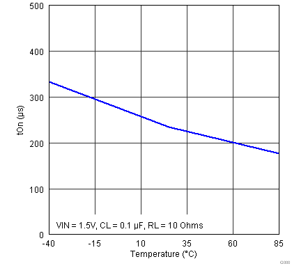 Figure 35. Turn-on Time vs Temperature
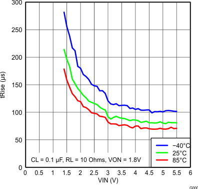 Figure 37. Rise Time vs Input Voltage
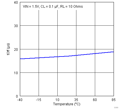 Figure 36. Turn-off Time vs Temperature
8.11 Typical AC Characteristics, TPS22913C
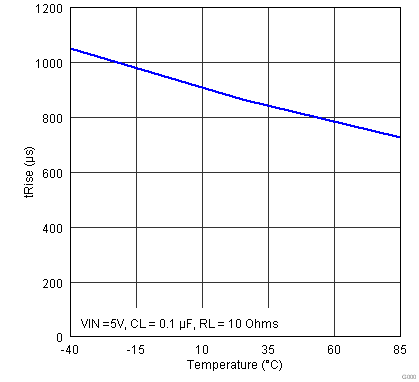
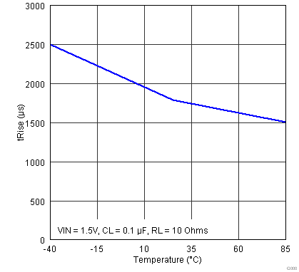
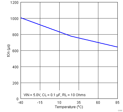
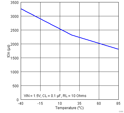 Figure 44. Turn-On Time vs Temperature
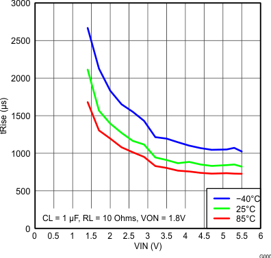 Figure 46. Rise Time vs Input Voltage
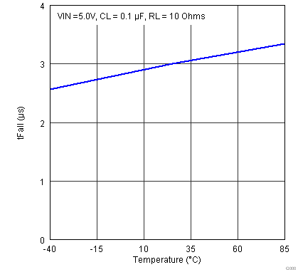
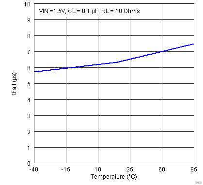

 Figure 45. Turn-Off Time vs Temperature