SLVSB34A October 2011 – June 2015 TPS22933
PRODUCTION DATA.
- 1 Features
- 2 Applications
- 3 Description
- 4 Revision History
- 5 Pin Configuration and Functions
- 6 Specifications
- 7 Parametric Measurement Information
- 8 Detailed Description
- 9 Application and Implementation
- 10Power Supply Recommendations
- 11Layout
- 12Device and Documentation Support
- 13Mechanical, Packaging, and Orderable Information
8 Detailed Description
8.1 Overview
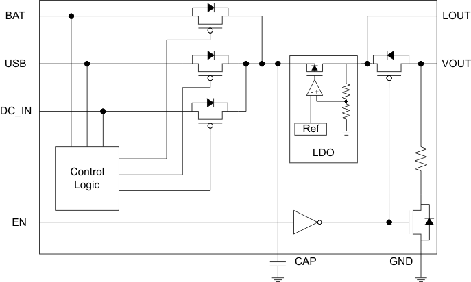
The TPS22933 is a triple-input power multiplexer with auto-input selection and a low dropout linear regulator. The device contains three P-channel MOSFETs that can operate over an input voltage range of 2.5 V to 12 V. The TPS22933 automatically selects the highest voltage level (from BAT, USB, and DC_IN) and enables that input to source the LDO. LOUT is an always-on output from the LDO, but VOUT can be switched on and off using the EN pin.
8.2 Functional Block Diagram

8.3 Feature Description
8.3.1 ON and OFF Control
The EN pin controls the state of the VOUT switch and VOUT pulldown switch. EN has no control over LOUT. Asserting EN enables the VOUT switch and disables the Quick Output Discharge (QOD) switch. Deasserting EN disables the VOUT switch and enables the QOD switch. EN is active high and has a low threshold, making it capable of interfacing with low voltage signals. The EN pin is compatible with standard GPIO Logic threshold and can be used with any microcontroller with 1.2-V, 1.8-V, 2.5-V or 3.3-V GPIOs.
8.3.2 Power Changeover
The TPS22933 LDO is powered by the highest level input. When input voltages change, the TPS22933 may change which input powers the LDO. During initial power up, the input that reaches the highest value first will power the LDO. Once that decision is made, changing between input sources is based on VCO. When an input source becomes VCO over the input currently supplying power to the LDO, changeover will occur and the new, higher input will power the LDO.
8.4 Device Functional Modes
Table 2 and Table 3 show the behavior of the device with various voltage conditions for the inputs and enable pin.
Table 2. Function Table
| EN | LDO TO LOUT | LDO TO VOUT | VOUT TO GND | |
|---|---|---|---|---|
| L | ON | OFF | ON | |
| H | ON | ON | OFF | |
Table 3. Input Selection Table (V1 > V2 > V3)
| BAT | USB | DC_IN | LDO SUPPLY | |
|---|---|---|---|---|
| V1 | V2 or V3 | V2 or V3 | BAT | |
| V2 or V3 | V1 | V2 or V3 | USB | |
| V2 or V3 | V2 or V3 | V1 | DC_IN | |
| V1 | V1 | V1 | See (1) | |