SLVSBS6A June   2013  – January 2015 TPS22963C , TPS22964C

PRODUCTION DATA.  

  1. Features
  2. Applications
  3. Description
  4. Simplified Schematic
  5. Revision History
  6. Device Comparison Table
  7. Pin Configuration and Functions
  8. Specifications
    1. 8.1 Absolute Maximum Ratings
    2. 8.2 ESD Ratings
    3. 8.3 Recommended Operating Conditions
    4. 8.4 Thermal Information
    5. 8.5 Electrical Characteristics
    6. 8.6 Switching Characteristics
    7. 8.7 Typical Electrical Characteristics
    8. 8.8 Typical Switching Characteristics
    9. 8.9 Typical AC Scope Captures at TA = 25ºC
  9. Parametric Measurement Information
  10. 10Detailed Description
    1. 10.1 Overview
    2. 10.2 Functional Block Diagram
    3. 10.3 Feature Description
      1. 10.3.1 On/Off Control
      2. 10.3.2 Quick Output Discharge
    4. 10.4 Device Functional Modes
  11. 11Application and Implementation
    1. 11.1 Application Information
      1. 11.1.1 Input Capacitor
      2. 11.1.2 Output Capacitor
      3. 11.1.3 Standby Power Reduction
      4. 11.1.4 Reverse Current Protection
      5. 11.1.5 Power Supply Sequencing Without a GPIO Input
    2. 11.2 Typical Application
      1. 11.2.1 Design Requirements
      2. 11.2.2 Detailed Design Procedure
        1. 11.2.2.1 Managing Inrush Current
      3. 11.2.3 Application Curves
  12. 12Power Supply Recommendations
  13. 13Layout
    1. 13.1 Layout Guidelines
    2. 13.2 Layout Example
  14. 14Device and Documentation Support
    1. 14.1 Related Links
    2. 14.2 Trademarks
    3. 14.3 Electrostatic Discharge Caution
    4. 14.4 Glossary
  15. 15Mechanical, Packaging, and Orderable Information

パッケージ・オプション

メカニカル・データ(パッケージ|ピン)
サーマルパッド・メカニカル・データ
発注情報

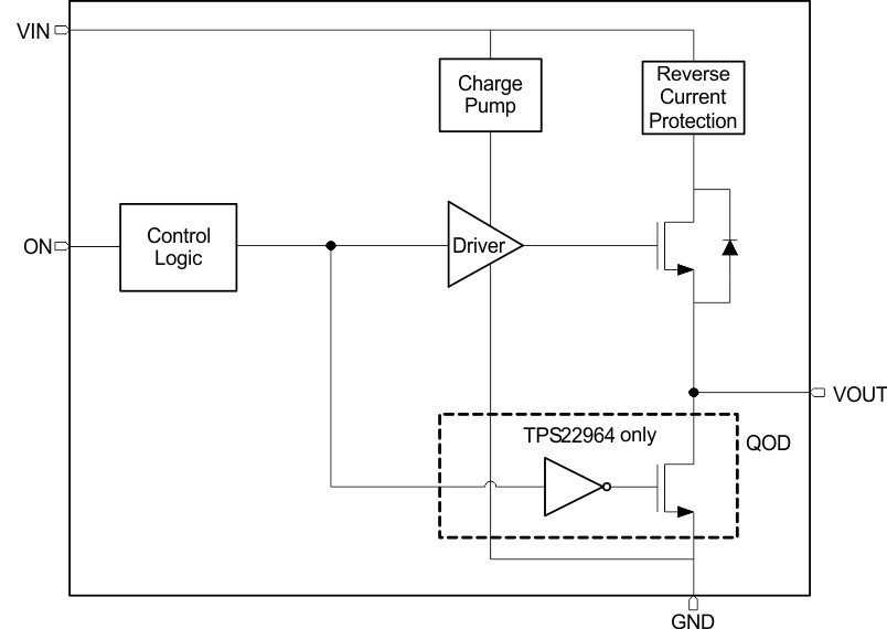
10 Detailed Description

10.1 Overview

The TPS22963/64 is a single channel, 3-A load switch in a small, space saving CSP-6 package. These devices implement an N-channel MOSFET to provide an ultra-low On-resistance for a low voltage drop across the device. A controlled rise time is used in applications to limit the inrush current.

10.2 Functional Block Diagram

bd_lvsbs6.gif

10.3 Feature Description

10.3.1 On/Off Control

The ON pin controls the state of the switch. It is an active “High” pin and has a low threshold making it capable of interfacing with low voltage GPIO control signals. It can be used with any microcontroller with 1.2 V, 1.8 V, 2.5 V, 3.3 V or 5.5 V GPIOs. Applying VIH on the ON pin will put the switch in the ON-state and VIL will put the switch in the OFF-state.

10.3.2 Quick Output Discharge

The TPS22964 includes the Quick Output Discharge (QOD) feature. When the switch is disabled, a discharge resistance with a typical value of 273Ω is connected between the output and ground. This resistance pulls down the output and prevents it from floating when the device is disabled.

10.4 Device Functional Modes

Table 1. Function Table

ON VIN to VOUT OUTPUT DISCHARGE(1)(2)
L OFF ACTIVE
H ON DISABLED
(1) This feature discharges the output of the switch to ground through a 273 Ω resistor, preventing the output from floating.
(2) This feature is in the TPS22964 device only (not in the TPS22963).