SLVSBS6A June 2013 – January 2015 TPS22963C , TPS22964C
PRODUCTION DATA.
- 1 Features
- 2 Applications
- 3 Description
- 4 Simplified Schematic
- 5 Revision History
- 6 Device Comparison Table
- 7 Pin Configuration and Functions
- 8 Specifications
- 9 Parametric Measurement Information
- 10Detailed Description
- 11Application and Implementation
- 12Power Supply Recommendations
- 13Layout
- 14Device and Documentation Support
- 15Mechanical, Packaging, and Orderable Information
13 Layout
13.1 Layout Guidelines
For best performance, all traces should be as short as possible. To be most effective, the input and output capacitors should be placed close to the device to minimize the effects that parasitic trace inductances may have on normal operation. Using wide traces for VIN, VOUT and GND will help minimize the parasitic electrical effects.
For higher reliability, the maximum IC junction temperature, TJ(max), should be restricted to 125˚C under normal operating conditions. Junction temperature is directly proportional to power dissipation in the device and the two are related by Equation 4.
Equation 4. 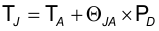
where
- TJ = Junction temperature of the device
- TA = Ambient temperature
- PD = Power dissipation inside the device
- ӨJA = Junction to ambient thermal resistance. See Thermal Information section of the datasheet. This parameter is highly dependent on board layout.
13.2 Layout Example
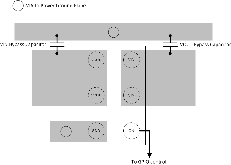 Figure 43. Layout Example