JAJSIF0E April   2014  – July 2022 TPS22965-Q1

PRODUCTION DATA  

  1. 特長
  2. アプリケーション
  3. 概要
  4. Revision History
  5. Device Comparison Table
  6. Pin Configuration and Functions
  7. Specifications
    1. 7.1 Absolute Maximum Ratings
    2. 7.2 ESD Ratings
    3. 7.3 Recommended Operating Conditions
    4. 7.4 Thermal Information
    5. 7.5 Electrical Characteristics—VBIAS = 5 V
    6. 7.6 Electrical Characteristics—VBIAS = 2.5 V
    7. 7.7 Switching Characteristics
    8. 7.8 Typical Characteristics
      1. 7.8.1 Typical DC Characteristics
      2. 7.8.2 Typical Switching Characteristics
  8. Parameter Measurement Information
  9. Detailed Description
    1. 9.1 Overview
    2. 9.2 Functional Block Diagram
    3. 9.3 Feature Description
      1. 9.3.1 Adjustable Rise Time
      2. 9.3.2 Quick Output Discharge (TPS22965-Q1 and TPS22965W-Q1 Only)
      3. 9.3.3 Low Power Consumption During OFF State
    4. 9.4 Device Functional Modes
  10. 10Application and Implementation
    1. 10.1 Application Information
      1. 10.1.1 VIN to VOUT Voltage Drop
      2. 10.1.2 On and Off Control
      3. 10.1.3 Input Capacitor (Optional)
      4. 10.1.4 Output Capacitor (Optional)
      5. 10.1.5 VIN and VBIAS Voltage Range
    2. 10.2 Typical Application
      1. 10.2.1 Design Requirements
      2. 10.2.2 Detailed Design Procedure
        1. 10.2.2.1 Inrush Current
      3. 10.2.3 Application Curves
  11. 11Power Supply Recommendations
  12. 12Layout
    1. 12.1 Layout Guidelines
    2. 12.2 Layout Example
    3. 12.3 Thermal Consideration
  13. 13Device and Documentation Support
    1. 13.1 Documentation Support
      1. 13.1.1 Related Documentation
    2. 13.2 Receiving Notification of Documentation Updates
    3. 13.3 サポート・リソース
    4. 13.4 Trademarks
    5. 13.5 Electrostatic Discharge Caution
    6. 13.6 Glossary
  14. 14Mechanical, Packaging, and Orderable Information

パッケージ・オプション

メカニカル・データ(パッケージ|ピン)
サーマルパッド・メカニカル・データ
発注情報

VIN to VOUT Voltage Drop

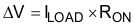
The VIN to VOUT voltage drop in the device is determined by the RON of the device and the load current. The RON of the device depends upon the VIN and VBIAS conditions of the device. Refer to the RON specification of the device in the Electrical Characteristics—VBIAS = 2 V to 2.5 V table of this data sheet. After the RON of the device is determined based upon the VIN and VBIAS conditions, use the following equation to calculate the VIN to VOUT voltage drop.

Equation 2. GUID-0105E312-E7F1-4CA8-8870-1725B7AE270E-low.gif

where

  • ΔV = voltage drop from VIN to VOUT.
  • ILOAD = load current.
  • RON = On-resistance of the device for a specific VIN and VBIAS combination.

An appropriate ILOAD must be chosen such that the IMAX specification of the device is not violated.