JAJSJS0A June 2020 – September 2020 TPS23734
PRODUCTION DATA
- 1 特長
- 2 アプリケーション
- 3 概要
- 4 Revision History
- 5 Device Comparison Table
- 6 Pin Configuration and Functions
- 7 Specifications
-
8 Detailed Description
- 8.1 Overview
- 8.2 Functional Block Diagram
- 8.3
Feature Description
- 8.3.1 CLS Classification
- 8.3.2 DEN Detection and Enable
- 8.3.3 APD Auxiliary Power Detect
- 8.3.4 Internal Pass MOSFET
- 8.3.5 T2P and APDO Indicators
- 8.3.6
DC-DC Controller Features
- 8.3.6.1 VCC, VB, VBG and Advanced PWM Startup
- 28
- 8.3.6.2 CS, Current Slope Compensation and blanking
- 8.3.6.3 COMP, FB, EA_DIS, CP, PSRS and Opto-less Feedback
- 8.3.6.4 FRS Frequency Setting and Synchronization
- 8.3.6.5 DTHR and Frequency Dithering for Spread Spectrum Applications
- 8.3.6.6 SST and Soft-Start of the Switcher
- 8.3.6.7 SST, I_STP, LINEUV and Soft-Stop of the Switcher
- 8.3.7 Switching FET Driver - GATE, GTA2, DT
- 8.3.8 EMPS and Automatic MPS
- 8.3.9 VDD Supply Voltage
- 8.3.10 RTN, AGND, GND
- 8.3.11 VSS
- 8.3.12 Exposed Thermal pads - PAD_G and PAD_S
- 8.4
Device Functional Modes
- 8.4.1 PoE Overview
- 8.4.2 Threshold Voltages
- 8.4.3 PoE Start-Up Sequence
- 8.4.4 Detection
- 8.4.5 Hardware Classification
- 8.4.6 Maintain Power Signature (MPS)
- 8.4.7 Advanced Start-Up and Converter Operation
- 8.4.8 Line Undervoltage Protection and Converter Operation
- 8.4.9 PD Self-Protection
- 8.4.10 Thermal Shutdown - DC-DC Controller
- 8.4.11 Adapter ORing
-
9 Application and Implementation
- 9.1 Application Information
- 9.2
Typical Application
- 9.2.1
Design Requirements
- 9.2.1.1
Detailed Design Procedure
- 9.2.1.1.1 Input Bridges and Schottky Diodes
- 9.2.1.1.2 Input TVS Protection
- 9.2.1.1.3 Input Bypass Capacitor
- 9.2.1.1.4 Detection Resistor, RDEN
- 9.2.1.1.5 Classification Resistor, RCLS.
- 9.2.1.1.6 Dead Time Resistor, RDT
- 9.2.1.1.7 APD Pin Divider Network, RAPD1, RAPD2
- 9.2.1.1.8 Setting Frequency (RFRS) and Synchronization
- 9.2.1.1.9 Bias Supply Requirements and CVCC
- 9.2.1.1.10 APDO, T2P Interface
- 9.2.1.1.11 Secondary Soft Start
- 9.2.1.1.12 Frequency Dithering for Conducted Emissions Control
- 9.2.1.1
Detailed Design Procedure
- 9.2.1
Design Requirements
- 10Power Supply Recommendations
- 11Layout
- 12Device and Documentation Support
- 13Mechanical, Packaging, and Orderable Information
9.2.1.1.6 Dead Time Resistor, RDT
Program the dead time with a resistor connected from DT to RTN. The required dead-time period depends on the specific topology and parasitics. The easiest technique to obtain the optimum timing resistor is to build the supply. A good initial value is 100 ns. Then the dead time can be tuned to achieve the best efficiency after considering all corners of operation (load, input voltage, and temperature).
- Choose RDT as follows assuming a tDT of 100 ns:
-
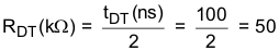
- Choose RDT = 49.9 kΩ
-