JAJSFJ2G March 2018 – August 2020 TPS23880
PRODUCTION DATA
- 1 特長
- 2 アプリケーション
- 3 概要
- 4 Revision History
- 5 Device Comparison Table
- 6 Pin Configuration and Functions
- 7 Specifications
- 8 Parameter Measurement Information
-
9 Detailed Description
- 9.1 Overview
- 9.2 Functional Block Diagram
- 9.3 Feature Description
- 9.4 Device Functional Modes
- 9.5 I2C Programming
- 9.6
Register Maps
- 9.6.1 Complete Register Set
- 9.6.2
Detailed Register Descriptions
- 9.6.2.1 INTERRUPT Register
- 9.6.2.2 INTERRUPT MASK Register
- 9.6.2.3 POWER EVENT Register
- 9.6.2.4 DETECTION EVENT Register
- 9.6.2.5 FAULT EVENT Register
- 9.6.2.6 START/ILIM EVENT Register
- 9.6.2.7 SUPPLY and FAULT EVENT Register
- 9.6.2.8 CHANNEL 1 DISCOVERY Register
- 9.6.2.9 CHANNEL 2 DISCOVERY Register
- 9.6.2.10 CHANNEL 3 DISCOVERY Register
- 9.6.2.11 CHANNEL 4 DISCOVERY Register
- 9.6.2.12 POWER STATUS Register
- 9.6.2.13 PIN STATUS Register
- 9.6.2.14 OPERATING MODE Register
- 9.6.2.15 DISCONNECT ENABLE Register
- 9.6.2.16 DETECT/CLASS ENABLE Register
- 9.6.2.17 Power Priority / 2Pair PCUT Disable Register Name
- 9.6.2.18 TIMING CONFIGURATION Register
- 9.6.2.19 GENERAL MASK Register
- 9.6.2.20 DETECT/CLASS RESTART Register
- 9.6.2.21 POWER ENABLE Register
- 9.6.2.22 RESET Register
- 9.6.2.23 ID Register
- 9.6.2.24 Connection Check and Auto Class Status Register
- 9.6.2.25 2-Pair Police Ch-1 Configuration Register
- 9.6.2.26 2-Pair Police Ch-2 Configuration Register
- 9.6.2.27 2-Pair Police Ch-3 Configuration Register
- 9.6.2.28 2-Pair Police Ch-4 Configuration Register
- 9.6.2.29 Power-on Fault Register
- 9.6.2.30 PORT RE-MAPPING Register
- 9.6.2.31 Channels 1 and 2 Multi Bit Priority Register
- 9.6.2.32 Channels 3 and 4 Multi Bit Priority Register
- 9.6.2.33 4-Pair Wired and Port Power Allocation Register
- 9.6.2.34 4-Pair Police Ch-1 and 2 Configuration Register
- 9.6.2.35 4-Pair Police Ch-3 and 4 Configuration Register
- 9.6.2.36 TEMPERATURE Register
- 9.6.2.37 4-Pair Fault Configuration Register
- 9.6.2.38 INPUT VOLTAGE Register
- 9.6.2.39 CHANNEL 1 CURRENT Register
- 9.6.2.40 CHANNEL 2 CURRENT Register
- 9.6.2.41 CHANNEL 3 CURRENT Register
- 9.6.2.42 CHANNEL 4 CURRENT Register
- 9.6.2.43 CHANNEL 1 VOLTAGE Register
- 9.6.2.44 CHANNEL 2 VOLTAGE Register
- 9.6.2.45 CHANNEL 3 VOLTAGE Register
- 9.6.2.46 CHANNEL 4 VOLTAGE Register
- 9.6.2.47 2x FOLDBACK SELECTION Register
- 97
- 9.6.2.48 FIRMWARE REVISION Register
- 9.6.2.49 I2C WATCHDOG Register
- 9.6.2.50 DEVICE ID Register
- 9.6.2.51 CHANNEL 1 DETECT RESISTANCE Register
- 9.6.2.52 CHANNEL 2 DETECT RESISTANCE Register
- 9.6.2.53 CHANNEL 3 DETECT RESISTANCE Register
- 9.6.2.54 CHANNEL 4 DETECT RESISTANCE Register
- 9.6.2.55 CHANNEL 1 ASSIGNED CLASS Register
- 9.6.2.56 CHANNEL 2 ASSIGNED CLASS Register
- 9.6.2.57 CHANNEL 3 ASSIGNED CLASS Register
- 9.6.2.58 CHANNEL 4 ASSIGNED CLASS Register
- 9.6.2.59 AUTO CLASS CONTROL Register
- 9.6.2.60 CHANNEL 1 AUTO CLASS POWER Register
- 9.6.2.61 CHANNEL 2 AUTO CLASS POWER Register
- 9.6.2.62 CHANNEL 3 AUTO CLASS POWER Register
- 9.6.2.63 CHANNEL 4 AUTO CLASS POWER Register
- 9.6.2.64 ALTERNATIVE FOLDBACK Register
- 9.6.2.65 SRAM CONTROL Register
- 10Application and Implementation
- 11Power Supply Recommendations
- 12Layout
- 13Device and Documentation Support
- 14Mechanical, Packaging, and Orderable Information
パッケージ・オプション
メカニカル・データ(パッケージ|ピン)
- RTQ|56
サーマルパッド・メカニカル・データ
- RTQ|56
発注情報
10.2.3 Application Curves
Unless otherwise noted, measurements taken on the TPS23880 EVM and Sifos PSA-3000
PowerSync Analyzer with PSA3202 test cards. Test conditions are
TJ = 25 °C, VVDD = 3.3 V, VVPWR = 54
V, VDGND = VAGND, DGND, KSENSA, KSENSB, KSENSC and
KSENSD connected to AGND, and all outputs are unloaded, 2xFBn = 0. Positive
currents are into pins. RS = 0.255 Ω, to KSENSA (SEN1 or SEN2), to KSENSB (SEN3 or SEN4), to
KSENSC (SEN5 or SEN6) or to KSENSD (SEN7 or SEN8). All voltages are with
respect to AGND unless otherwise noted. Operating registers loaded with
default values unless otherwise noted.
Unless otherwise noted, measurements taken on the TPS23880 EVM and Sifos PSA-3000
PowerSync Analyzer with PSA3202 test cards. Test conditions are
TJ = 25 °C, VVDD = 3.3 V, VVPWR = 54
V, VDGND = VAGND, DGND, KSENSA, KSENSB, KSENSC and
KSENSD connected to AGND, and all outputs are unloaded, 2xFBn = 0. Positive
currents are into pins. RS = 0.255 Ω, to KSENSA (SEN1 or SEN2), to KSENSB (SEN3 or SEN4), to
KSENSC (SEN5 or SEN6) or to KSENSD (SEN7 or SEN8). All voltages are with
respect to AGND unless otherwise noted. Operating registers loaded with
default values unless otherwise noted.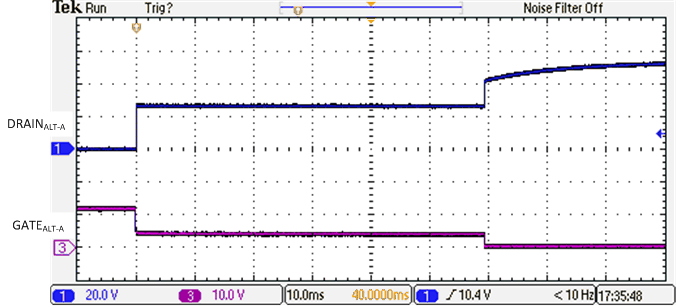 Figure 10-4 2-Pair
ILIM Foldback and Turn Off. Unless otherwise noted, measurements taken on the TPS23880 EVM and Sifos PSA-3000
PowerSync Analyzer with PSA3202 test cards. Test conditions are
TJ = 25 °C, VVDD = 3.3 V, VVPWR = 54
V, VDGND = VAGND, DGND, KSENSA, KSENSB, KSENSC and
KSENSD connected to AGND, and all outputs are unloaded, 2xFBn = 0. Positive
currents are into pins. RS = 0.255 Ω, to KSENSA (SEN1 or SEN2), to KSENSB (SEN3 or SEN4), to
KSENSC (SEN5 or SEN6) or to KSENSD (SEN7 or SEN8). All voltages are with
respect to AGND unless otherwise noted. Operating registers loaded with
default values unless otherwise noted.
 Figure 10-4 2-Pair
ILIM Foldback and Turn Off. Unless otherwise noted, measurements taken on the TPS23880 EVM and Sifos PSA-3000
PowerSync Analyzer with PSA3202 test cards. Test conditions are
TJ = 25 °C, VVDD = 3.3 V, VVPWR = 54
V, VDGND = VAGND, DGND, KSENSA, KSENSB, KSENSC and
KSENSD connected to AGND, and all outputs are unloaded, 2xFBn = 0. Positive
currents are into pins. RS = 0.255 Ω, to KSENSA (SEN1 or SEN2), to KSENSB (SEN3 or SEN4), to
KSENSC (SEN5 or SEN6) or to KSENSD (SEN7 or SEN8). All voltages are with
respect to AGND unless otherwise noted. Operating registers loaded with
default values unless otherwise noted.
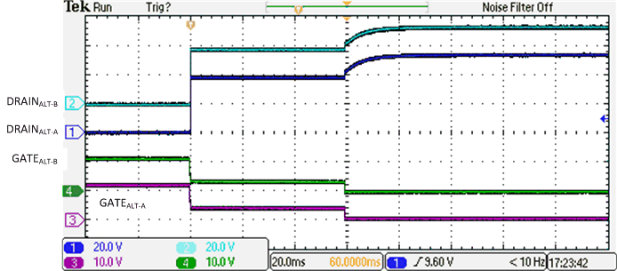 Figure 10-6 4-Pair ILIM Foldback and Turn Off
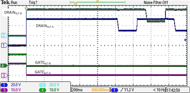 Figure 10-8 4-Pair Backoff Due to 4PPCut Fault
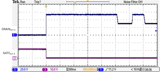 Figure 10-5 2-Pair Backoff
due to PCut Fault
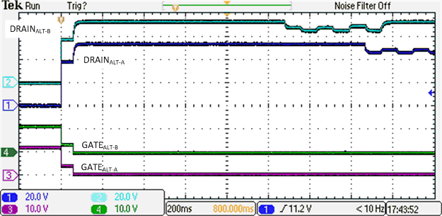 Figure 10-7 4-Pair Backoff Due to ILIM Fault
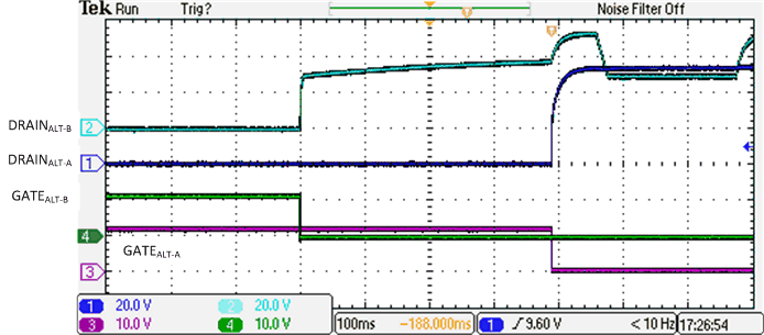 Figure 10-9 4-Pair Single Signature Class 0-4 Disconnect
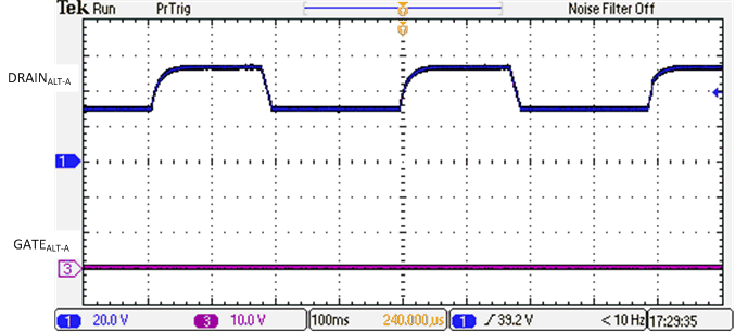 Figure 10-10 2-Pair Open
Circuit Detection Signature
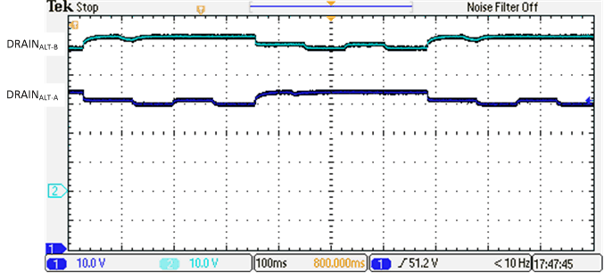 Figure 10-12 4-Pair Low Resistance (11kΩ) Detection Signature
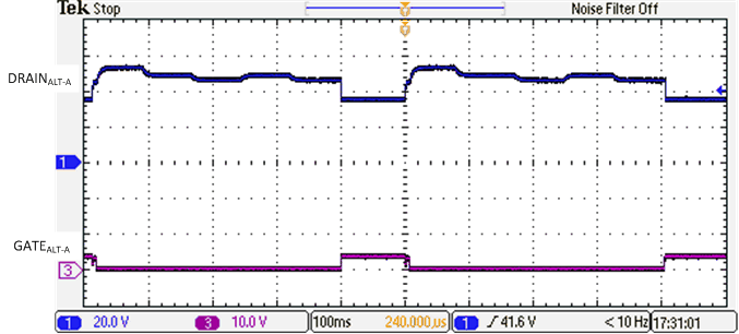 Figure 10-14 2-Pair
Semi-Auto Mode Discovery with a Valid Class 0-3 Load
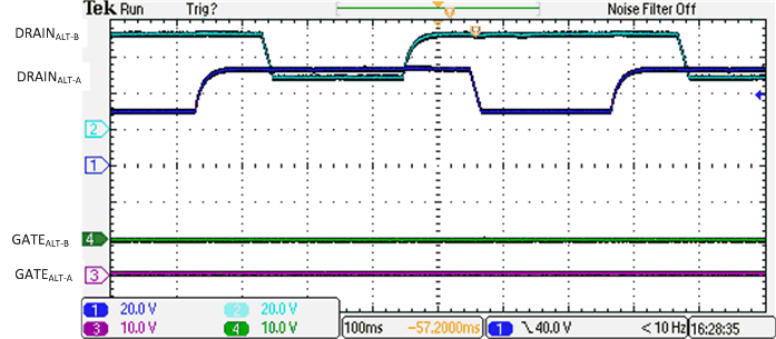 Figure 10-11 4-Pair Open Circuit Detection Signature
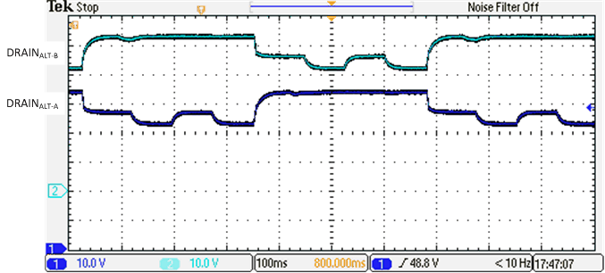 Figure 10-13 4-Pair High Resistance (36kΩ) Detection Signature
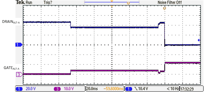 Figure 10-15 2-Pair 1-Finger
Classification and Turn On
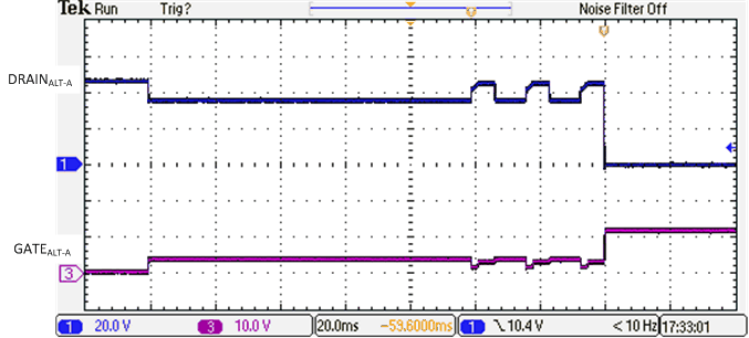 Figure 10-16 2-Pair 3-Finger
Classification and Turn On
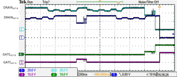 Figure 10-18 4-Pair Single Signature Discovery and Turn On from Semi-Auto Mode
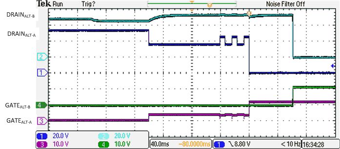 Figure 10-20 4-Pair Single Signature 3-Finger Classification and Turn On
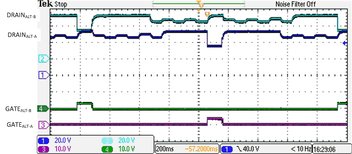 Figure 10-17 4-Pair Semi-Auto Mode Discovery with a Valid Single Signature Class 0-3
Load
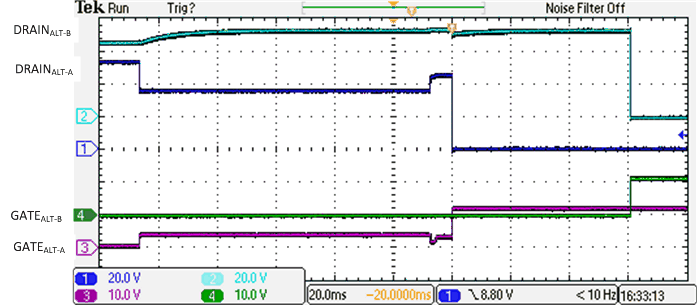 Figure 10-19 4-Pair Single Signature 1-Finger Classification and Turn On
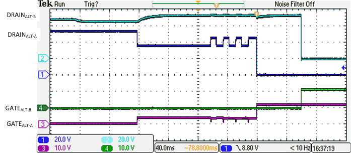 Figure 10-21 4-Pair Single Signature 4-Finger Classification and Turn On
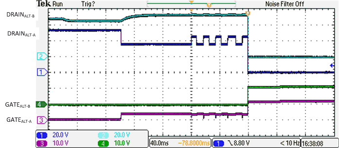 Figure 10-22 4-Pair Single Signature 5-Finger Classification and Turn On
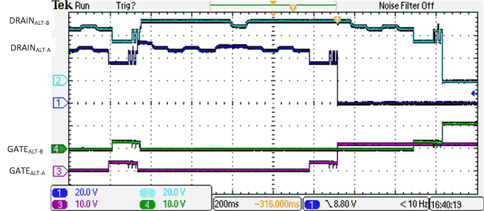 Figure 10-24 4-Pair Dual Signature Discovery and Turn On from Semi-Auto Mode
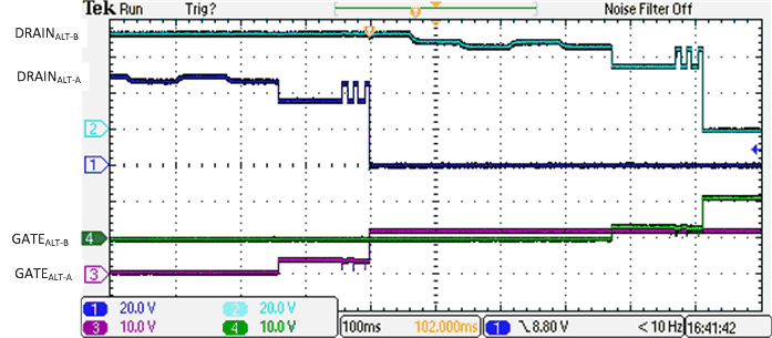 Figure 10-26 4-Pair Dual Signature 3-Finger Classification and Turn On
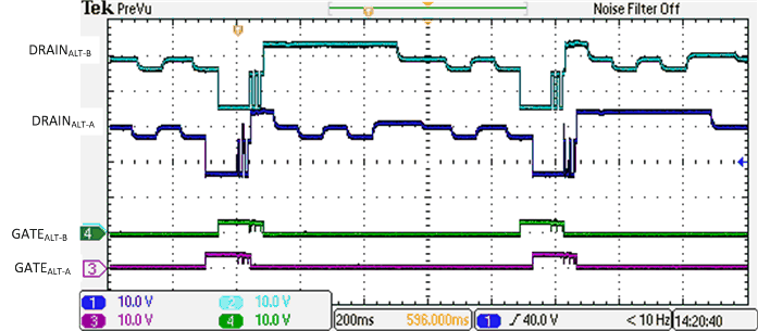 Figure 10-23 4-Pair Semi-Auto Mode Discovery with a Valid Dual Signature Class 4D
Load
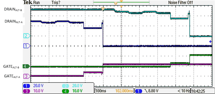 Figure 10-25 4-Pair Dual Signature 1-Finger Classification and Turn On
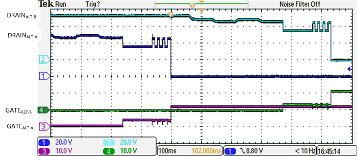 Figure 10-27 4-Pair Dual Signature 4-Finger Classification and Turn On