JAJSHI6G June 2018 – July 2021 TPS25830-Q1 , TPS25831-Q1
PRODUCTION DATA
- 1 特長
- 2 アプリケーション
- 3 概要
- 4 Revision History
- 5 概要 (続き)
- 6 Device Comparison Table
- 7 Pin Configuration and Functions
- 8 Specifications
- 9 Parameter Measurement Information
-
10Detailed Description
- 10.1 Overview
- 10.2 Functional Block Diagram
- 10.3
Feature Description
- 10.3.1 Buck Regulator
- 10.3.2 Enable/UVLO and Start-up
- 10.3.3 Switching Frequency and Synchronization (RT/SYNC)
- 10.3.4 Spread-Spectrum Operation
- 10.3.5 VCC, VCC_UVLO
- 10.3.6 Minimum ON-time, Minimum OFF-time
- 10.3.7 Internal Compensation
- 10.3.8 Bootstrap Voltage (BOOT)
- 10.3.9 RSNS, RSET, RILIMIT and RIMON
- 10.3.10 Overcurrent and Short Circuit Protection
- 10.3.11 Overvoltage, IEC and Short to Battery Protection
- 10.3.12 Cable Compensation
- 10.3.13 USB Port Control
- 10.3.14 FAULT Response
- 10.3.15 USB Specification Overview
- 10.3.16 USB Type-C® Basics
- 10.3.17 Device Power Pins (IN, CSN/OUT, and PGND)
- 10.3.18 Thermal Shutdown
- 10.3.19 Power Wake
- 10.3.20 Thermal Sensing with NTC (TPS25831-Q1)
- 10.4
Device Functional Modes
- 10.4.1 Shutdown Mode
- 10.4.2 Standby Mode
- 10.4.3 Active Mode
- 10.4.4 Device Truth Table (TT)
- 10.4.5 USB Port Operating Modes
- 10.4.6 High-Bandwidth Data-Line Switches (TPS25830-Q1 only)
-
11Application and Implementation
- 11.1 Application Information
- 11.2
Typical Application
- 11.2.1 Design Requirements
- 11.2.2
Detailed Design Procedure
- 11.2.2.1 Output Voltage
- 11.2.2.2 Switching Frequency
- 11.2.2.3 Inductor Selection
- 11.2.2.4 Output Capacitor Selection
- 11.2.2.5 Input Capacitor Selection
- 11.2.2.6 Bootstrap Capacitor Selection
- 11.2.2.7 VCC Capacitor Selection
- 11.2.2.8 Enable and Undervoltage Lockout Set-Point
- 11.2.2.9 Current Limit Set-Point
- 11.2.2.10 Cable Compensation Set-Point
- 11.2.2.11 LD_DET, POL, and FAULT Resistor Selection
- 11.2.3 Application Curves
- 12Power Supply Recommendations
- 13Layout
- 14Device and Documentation Support
- 15Mechanical, Packaging, and Orderable Information
パッケージ・オプション
メカニカル・データ(パッケージ|ピン)
- RHB|32
サーマルパッド・メカニカル・データ
- RHB|32
発注情報
11.2.2.4 Output Capacitor Selection
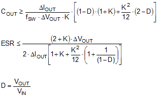
The value of the output capacitor, and its ESR, determine the output voltage ripple and load transient performance. The output capacitor bank is usually limited by the load transient requirements, rather than the output voltage ripple. Equation 11 can be used to estimate a lower bound on the total output capacitance, and an upper bound on the ESR, required to meet a specified load transient.
where
- ΔVOUT = output voltage transient
- ΔIOUT = output current transient
- K = Ripple factor from Inductor Selection
Once the output capacitor and ESR have been calculated, Equation 12 can be used to check the peak-to-peak output voltage ripple; Vr.
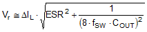
The output capacitor and ESR can then be adjusted to meet both the load transient and output ripple requirements.
For this example we require a ΔVOUT of ≤ 250 mV for an output current step of ΔIOUT = 2.7 A. Equation 11 gives a minimum value of 86 µF and a maximum ESR of 0.08 Ω. Assuming a 20% tolerance and a 10% bias de-rating, we arrive at a minimum capacitance of 110 µF. This can be achieved with a bank of 5 × 22-µF, 10-V, ceramic capacitors in the 1210 case size. More output capacitance can be used to improve the load transient response. Ceramic capacitors can easily meet the minimum ESR requirements. In some cases an aluminum electrolytic capacitor can be placed in parallel with the ceramics to help build up the required value of capacitance.
In practice the output capacitor has the most influence on the transient response and loop phase margin. Load transient testing and Bode plots are the best way to validate any given design and should always be completed before the application goes into production. In addition to the required output capacitance, a small ceramic placed on the output can help to reduce high frequency noise. Small case size ceramic capacitors in the range of 1 nF to 100 nF can be very helpful in reducing voltage spikes on the output caused by inductor and board parasitics.
The maximum value of total output capacitance should be limited to about 10 times the design value, or 1000 µF, whichever is smaller. Large values of output capacitance can adversely affect the start-up behavior of the regulator as well as the loop stability. If values larger than noted here must be used, then a careful study of start-up at full load and loop stability must be performed.