JAJSHI6G June 2018 – July 2021 TPS25830-Q1 , TPS25831-Q1
PRODUCTION DATA
- 1 特長
- 2 アプリケーション
- 3 概要
- 4 Revision History
- 5 概要 (続き)
- 6 Device Comparison Table
- 7 Pin Configuration and Functions
- 8 Specifications
- 9 Parameter Measurement Information
-
10Detailed Description
- 10.1 Overview
- 10.2 Functional Block Diagram
- 10.3
Feature Description
- 10.3.1 Buck Regulator
- 10.3.2 Enable/UVLO and Start-up
- 10.3.3 Switching Frequency and Synchronization (RT/SYNC)
- 10.3.4 Spread-Spectrum Operation
- 10.3.5 VCC, VCC_UVLO
- 10.3.6 Minimum ON-time, Minimum OFF-time
- 10.3.7 Internal Compensation
- 10.3.8 Bootstrap Voltage (BOOT)
- 10.3.9 RSNS, RSET, RILIMIT and RIMON
- 10.3.10 Overcurrent and Short Circuit Protection
- 10.3.11 Overvoltage, IEC and Short to Battery Protection
- 10.3.12 Cable Compensation
- 10.3.13 USB Port Control
- 10.3.14 FAULT Response
- 10.3.15 USB Specification Overview
- 10.3.16 USB Type-C® Basics
- 10.3.17 Device Power Pins (IN, CSN/OUT, and PGND)
- 10.3.18 Thermal Shutdown
- 10.3.19 Power Wake
- 10.3.20 Thermal Sensing with NTC (TPS25831-Q1)
- 10.4
Device Functional Modes
- 10.4.1 Shutdown Mode
- 10.4.2 Standby Mode
- 10.4.3 Active Mode
- 10.4.4 Device Truth Table (TT)
- 10.4.5 USB Port Operating Modes
- 10.4.6 High-Bandwidth Data-Line Switches (TPS25830-Q1 only)
-
11Application and Implementation
- 11.1 Application Information
- 11.2
Typical Application
- 11.2.1 Design Requirements
- 11.2.2
Detailed Design Procedure
- 11.2.2.1 Output Voltage
- 11.2.2.2 Switching Frequency
- 11.2.2.3 Inductor Selection
- 11.2.2.4 Output Capacitor Selection
- 11.2.2.5 Input Capacitor Selection
- 11.2.2.6 Bootstrap Capacitor Selection
- 11.2.2.7 VCC Capacitor Selection
- 11.2.2.8 Enable and Undervoltage Lockout Set-Point
- 11.2.2.9 Current Limit Set-Point
- 11.2.2.10 Cable Compensation Set-Point
- 11.2.2.11 LD_DET, POL, and FAULT Resistor Selection
- 11.2.3 Application Curves
- 12Power Supply Recommendations
- 13Layout
- 14Device and Documentation Support
- 15Mechanical, Packaging, and Orderable Information
パッケージ・オプション
メカニカル・データ(パッケージ|ピン)
- RHB|32
サーマルパッド・メカニカル・データ
- RHB|32
発注情報
10.3.12 Cable Compensation
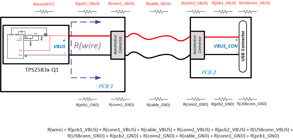
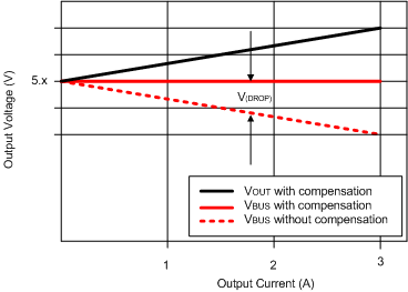
When a load draws current through a long or thin wire, there is an IR drop that reduces the voltage delivered to the load. Cable droop compensation linearly increases the voltage at the CSN/OUT pin of TPS2583x-Q1 as load current increases with the objective of maintaining VBUS_CON (the bus voltage at the USB connector) at 5 V, regardless of load conditions. Most portable devices charge at maximum current when 5 V is present at the USB connector. Figure 10-22 provides an example of resistor drops encountered when designing an automotive USB system with a remote USB connector location.
 Figure 10-22 Automotive USB Resistances
The TPS2583x-Q1 detects the load current and increases the voltage at the CSN/OUT pin to compensate the IR drop in the charging path according to the gain set by the RSNS, RSET, and RIMON resistors as described in RSNS, RSET, RILIMIT, and RIMON.
The amount of cable droop compensation required can be estimated by the following equation ΔVOUT = (RSNS + RDSON_NFET + RWIRE) × IBUS. RIMON is then chosen by RIMON = (ΔVOUT × RSET × 2) / (IBUS × RSNS), where ΔVOUT is the desired cable droop compensation voltage at full load.
 Figure 10-23 Voltage Drop
Per RSNS, RSET, RILIMIT, and RIMON, in most cases, the recommended voltage across RSNS should be 50 mV. In type-C application, typical RIMON resistors value are listed in Table 10-3 given the condition full load current = 3 A, RSNS = 15 mΩ and RSET = 300 Ω.
| Cable Compensation Voltage at 3-A Full Load (V) | RIMON (kΩ) | |
|---|---|---|
| 0.3 | 4.02 | |
| 0.6 | 8.06 | |
| 0.9 | 12.1 | |
| 1.2 | 16.2 | |
| 1.5 | 20 | |
Pls be noted that the max cable compensation voltage in TPS2583x-Q1 is 1.5 V.