JAJSCF6G July   2016  – December  2019 TPS2660

PRODUCTION DATA.  

  1. 特長
  2. アプリケーション
    1.     概略回路図
  3. 概要
    1.     -60V電源における入力逆極性保護
  4. 改訂履歴
  5. 概要(続き)
  6. Device Comparison Table
  7. Pin Configuration and Functions
    1.     Pin Functions
  8. Specifications
    1. 8.1 Absolute Maximum Ratings
    2. 8.2 ESD Ratings
    3. 8.3 Recommended Operating Conditions
    4. 8.4 Thermal Information
    5. 8.5 Electrical Characteristics
    6. 8.6 Timing Requirements
    7. 8.7 Typical Characteristics
  9. Parameter Measurement Information
  10. 10Detailed Description
    1. 10.1 Overview
    2. 10.2 Functional Block Diagram
    3. 10.3 Feature Description
      1. 10.3.1 Undervoltage Lockout (UVLO)
      2. 10.3.2 Overvoltage Protection (OVP)
      3. 10.3.3 Reverse Input Supply Protection
      4. 10.3.4 Hot Plug-In and In-Rush Current Control
      5. 10.3.5 Overload and Short Circuit Protection
        1. 10.3.5.1 Overload Protection
          1. 10.3.5.1.1 Active Current Limiting
          2. 10.3.5.1.2 Electronic Circuit Breaker with Overload Timeout, MODE = OPEN
        2. 10.3.5.2 Short Circuit Protection
          1. 10.3.5.2.1 Start-Up With Short-Circuit On Output
        3. 10.3.5.3 FAULT Response
          1. 10.3.5.3.1 Look Ahead Overload Current Fault Indicator
        4. 10.3.5.4 Current Monitoring
        5. 10.3.5.5 IN, OUT, RTN, and GND Pins
        6. 10.3.5.6 Thermal Shutdown
        7. 10.3.5.7 Low Current Shutdown Control (SHDN)
    4. 10.4 Device Functional Modes
  11. 11Application and Implementation
    1. 11.1 Application Information
    2. 11.2 Typical Application
      1. 11.2.1 Design Requirements
      2. 11.2.2 Detailed Design Procedure
        1. 11.2.2.1 Step by Step Design Procedure
        2. 11.2.2.2 Programming the Current-Limit Threshold—R(ILIM) Selection
        3. 11.2.2.3 Undervoltage Lockout and Overvoltage Set Point
        4. 11.2.2.4 Programming Current Monitoring Resistor—RIMON
        5. 11.2.2.5 Setting Output Voltage Ramp Time—(tdVdT)
          1. 11.2.2.5.1 Case 1: Start-Up Without Load—Only Output Capacitance C(OUT) Draws Current During Start-Up
          2. 11.2.2.5.2 Case 2: Start-Up With Load—Output Capacitance C(OUT) and Load Draws Current During Start-Up
          3. 11.2.2.5.3 Support Component Selections—RFLTb and C(IN)
      3. 11.2.3 Application Curves
    3. 11.3 System Examples
      1. 11.3.1 Acive ORing Operation
      2. 11.3.2 Field Supply Protection in PLC, DCS I/O Modules
      3. 11.3.3 Simple 24-V Power Supply Path Protection
    4. 11.4 Do's and Don'ts
  12. 12Power Supply Recommendations
    1. 12.1 Transient Protection
  13. 13Layout
    1. 13.1 Layout Guidelines
    2. 13.2 Layout Example
  14. 14デバイスおよびドキュメントのサポート
    1. 14.1 デバイス・サポート
    2. 14.2 ドキュメントのサポート
      1. 14.2.1 関連資料
    3. 14.3 ドキュメントの更新通知を受け取る方法
    4. 14.4 コミュニティ・リソース
    5. 14.5 商標
    6. 14.6 静電気放電に関する注意事項
    7. 14.7 Glossary
  15. 15メカニカル、パッケージ、および注文情報

パッケージ・オプション

デバイスごとのパッケージ図は、PDF版データシートをご参照ください。

メカニカル・データ(パッケージ|ピン)
  • RHF|24
  • PWP|16
サーマルパッド・メカニカル・データ
発注情報

Short Circuit Protection

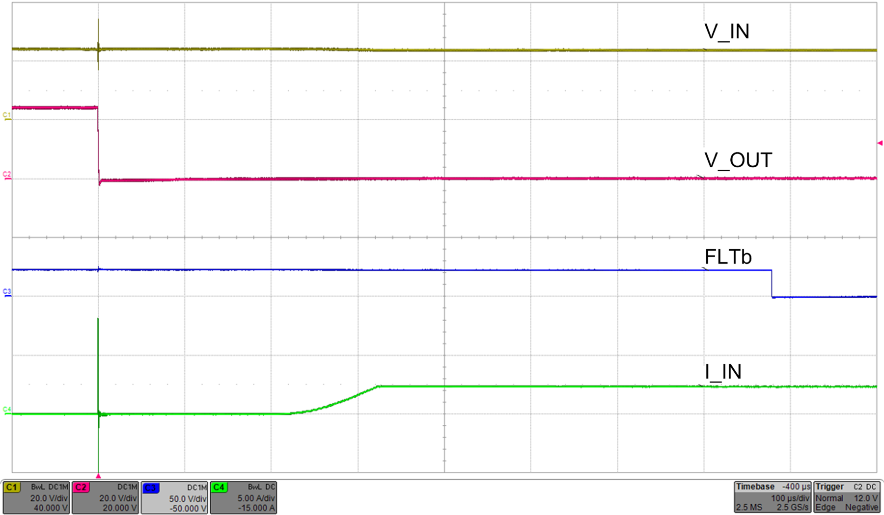
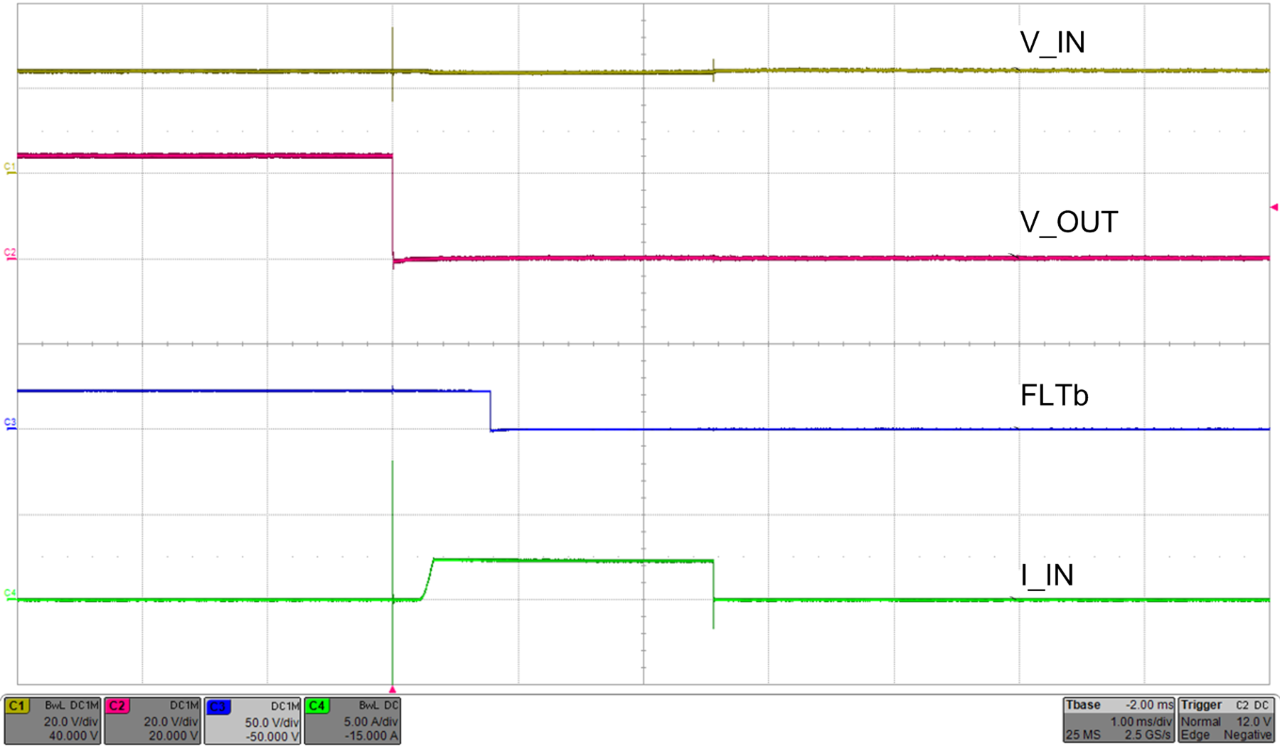
During a transient output short circuit event, the current through the device increases very rapidly. As the current-limit amplifier cannot respond quickly to this event due to its limited bandwidth, the device incorporates a fast-trip comparator, with a threshold I(FASTRIP). The fast-trip comparator turns off the internal FET within 250 ns (typical), when the current through the FET exceeds I(FASTRIP) (I(OUT) > I(FASTRIP)), and terminates the rapid short-circuit peak current. The fast-trip threshold is internally set to 87% higher than the programmed overload current limit (I(FASTRIP) = 1.87 × I(OL) + 0.015). The fast-trip circuit holds the internal FET off for only a few microseconds, after which the device turns back on slowly, allowing the current-limit loop to regulate the output current to I(OL). Then, device behaves similar to overload condition. Figure 43 and Figure 44 illustrate the behavior of the system when the current exceeds the fast-trip threshold.
TPS2660 scope_shot_15_slvsdg2.png
VIN = 24 V, RILIM = 5.36 kΩ
Figure 43. Output Hot Short Functionality at 24-V Input
TPS2660 scope_shot_16_slvsdg2.png
Figure 44. Zoomed at the Instance of Output Short