SLVSBR5C December 2012 – June 2015 TPS27082L
PRODUCTION DATA.
- 1 Features
- 2 Applications
- 3 Description
- 4 Revision History
- 5 Pin Configuration and Functions
- 6 Specifications
- 7 Detailed Description
-
8 Application and Implementation
- 8.1 Application Information
- 8.2 Typical Application
- 8.3
System Examples
- 8.3.1 TFT LCD Module Inrush Current Control
- 8.3.2 Standby Power Isolation
- 8.3.3 Boost Regulator With True Shutdown
- 8.3.4 Single Module Multiple Power Supply Sequencing
- 8.3.5 Multiple Modules Interdependent Power Supply Sequencing
- 8.3.6 Multiple Modules Interdependent Supply Sequencing Without a GPIO Input
- 9 Power Supply Recommendations
- 10Layout
- 11Device and Documentation Support
- 12Mechanical, Packaging, and Orderable Information
7 Detailed Description
7.1 Overview
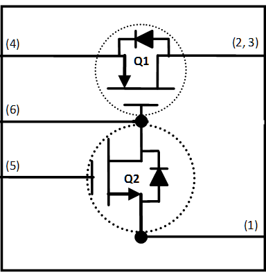
The TPS27082L IC is a high side load switch that integrates a Power PFET and its control circuit in a tiny TSOT-23 package. TPS27082L supports up to 8V supply input and up to 3A of load current. The TPS27082L can be used in a variety of applications. The device has a programmable slew rate which helps reduce or eliminate power supply droop due to large inrush currents. During shutdown, the device has very low leakage currents.
7.2 Functional Block Diagram

7.3 Feature Description
TPS27082L uses a low-voltage power PMOS transistor used as the pass element or switch between the supply and load. It also integrates an NMOS transistor to turn the PMOS on and off by interfacing with a wide range of GPIO voltages. Asserting an input voltage higher than Vih (1V) enables the PMOS switch by turning the NMOS and the NMOS driving the PMOS gate towards ground. Series resistance of 12.5 k connect at the source of NPN is integrated for TPS27082L. To control output rise time is programmed by connecting external capacitor at pin 6 of the device to design a delay time for PMOS to turn on.
7.4 Device Functional Modes
7.4.1 ON/OFF
When Vin > about 1 V and V(ON/OFF) > 1 V, the switch will turn on and Vout ≈ Vin.
When Vin > about 1 V and V(ON/OFF) < 1 V, the switch will turn off and Vout ≠ Vin.
7.4.2 Fastest Output Rise Time
Whenever it is desired to achieve the fastest output rise time, do not put a capacitor between Vout (Pins 2 and 3) and R1/C1 (pin 6).
7.4.3 Controlled Output Rise Time
Whenever it is desired to control the output rise time, tie pin 1 (R2) to a resistance (R2) and put a capacitor (C1) between Vout (Pins 2 and 3) and R1/C1 (pin 6).