JAJSET9B October 2017 – September 2019 TPS27S100
PRODUCTION DATA.
- 1 特長
- 2 アプリケーション
- 3 概要
- 4 改訂履歴
- 5 Pin Configuration and Functions
- 6 Specifications
- 7 Detailed Description
- 8 Application and Implementation
- 9 Power Supply Recommendations
- 10Layout
- 11デバイスおよびドキュメントのサポート
- 12メカニカル、パッケージ、および注文情報
パッケージ・オプション
メカニカル・データ(パッケージ|ピン)
サーマルパッド・メカニカル・データ
- PWP|14
発注情報
7.3.2 Adjustable Current Limit
A high-accuracy current limit allows high reliability of the design. It protects the load and the power supply from over-stressing during short-circuit-to-GND or power-up conditions. The current limit can also save system cost by reducing the size of PCB traces and connectors, and the capacity of the preceding power stage.
When the current-limit threshold is hit, a closed loop activates immediately. The output current is clamped at the set value, and a fault is reported out. The device heats up due to the high power dissipation on the power FET. If thermal shutdown occurs, the current limit is set to IILIM(TSD) to reduce the power dissipation on the power FET.
The device has two current-limit thresholds.
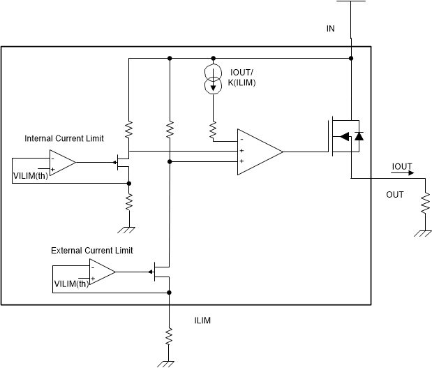
Internal current limit – The internal current limit is fixed at IILM(int). Tie the ILIM pin directly to the device GND for large-transient-current applications.
External adjustable current limit – An external resistor is used to set the current-limit threshold. Use Equation 2 below to calculate the RILIM. VILIM(th) is the internal band-gap voltage. K(ILIM) is the ratio of the output current and the current-limit set value. It is constant across the temperature and supply voltage. The external adjustable current limit allows the flexibility to set the current limit value by applications.

Note that if a GND network is used (which leads to the level shift between the device GND and board GND), the ILIM pin must be connected with device GND.
 Figure 26. Current-Limit Block Diagram
 For better protection from a hard short-to-GND condition (when the EN pin is enabled, a short to GND occurs suddenly), the device implements a fast-trip protection to turn off the channel before the current-limit closed loop is set up. The fast-trip response time is less than 1 μs, typically. With this fast response, the device can achieve better inrush current-suppression performance.