JAJSES3D December 2015 – December 2019 TPS2H160-Q1
PRODUCTION DATA.
- 1 特長
- 2 アプリケーション
- 3 概要
- 4 改訂履歴
- 5 Device Comparison Table
- 6 Pin Configuration and Functions
- 7 Specifications
-
8 Detailed Description
- 8.1 Overview
- 8.2 Functional Block Diagram
- 8.3 Feature Description
- 8.4 Device Functional Modes
- 9 Application and Implementation
- 10Power Supply Recommendations
- 11Layout
- 12デバイスおよびドキュメントのサポート
- 13メカニカル、パッケージ、および注文情報
パッケージ・オプション
メカニカル・データ(パッケージ|ピン)
- PWP|16
サーマルパッド・メカニカル・データ
- PWP|16
発注情報
7.6 Switching Characteristics
| PARAMETER | TEST CONDITIONS | MIN | TYP | MAX | UNIT | |
|---|---|---|---|---|---|---|
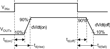
| td(on) | Delay time, VOUTx 10% after VINx↑ (See Figure 1.) | VVS = 13.5 V, VDIAG_EN = 5 V, IOUTx = 0.5 A, IN rising edge to 10% of VOUTx | 20 | 50 | 90 | µs |
| td(off) | Delay time, VOUTx 90% after VINx↓ (See Figure 1.) | VVS = 13.5 V, VDIAG_EN = 5 V, IOUTx = 0.5 A, IN falling edge to 90% of VOUTx | 20 | 50 | 90 | µs |
| dV/dt(on) | Turnon slew rate | VVS = 13.5 V, VDIAG_EN = 5 V, IOUTx = 0.5 A, VOUTx from 10% to 90% | 0.1 | 0.3 | 0.55 | V/µs |
| dV/dt(off) | Turnoff slew rate | VVS = 13.5 V, VDIAG_EN = 5 V, IOUTx = 0.5 A, VOUTx from 90% to 10% | 0.1 | 0.35 | 0.55 | V/µs |
| td(match) | td(rise) – td(fall) (See Figure 1.) | VVS = 13.5 V, IL = 0.5A. td, rise is the IN rising edge to VOUTx = 90%.
td(fall) is the IN falling edge to VOUTx = 10%. |
–50 | 50 | µs | |
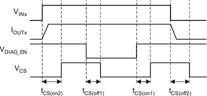
| CURRENT-SENSE CHARACTERISTICS (See Figure 2.) | ||||||
| tCS(off1) | CS settling time from DIAG_EN disabled(1) | VVS = 13.5 V, VINx = 5 V, IOUTx = 0.5 A. current limit = 2 A. DIAG_EN falling edge to 10% of VCS. | 20 | µs | ||
| tCS(on1) | CS settling time from DIAG_EN enabled(1) | VVS = 13.5 V, VINx = 5 V, IOUTx = 0.5 A. current limit is 2 A. DIAG_EN rising edge to 90% of VCS. | 20 | µs | ||
| tCS(off2) | CS settling time from IN falling edge | VVS = 13.5 V, VDIAG_EN = 5 V, IOUTx = 0.5 A. current limit = 2 A. IN falling edge to 10% of VCS | 20 | 100 | µs | |
| tCS(on2) | CS settling time from IN rising edge | VVS = 13.5 V, VDIAG_EN = 5 V, IOUTx = 0.5 A. current limit = 2 A. IN rising edge to 90% of VCS | 50 | 150 | µs | |
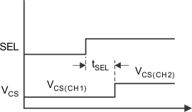
| tSEL | Multi-sense transition delay from channel to channel | VDIAG_EN = 5 V, current sense output delay when multi-sense pin SEL transitions from channel to channel | 50 | µs | ||
(1) Value specified by design, not subject to production test
 Figure 1. Output Delay Characteristics
  Figure 2. CS Delay Characteristics
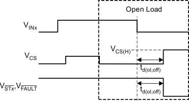
  Figure 3. Open-Load Blanking-Time Characteristics
  Figure 4. Multi-Sense Transition Delay