JAJSES3D December   2015  – December 2019 TPS2H160-Q1

PRODUCTION DATA.  

  1. 特長
  2. アプリケーション
  3. 概要
    1.     Device Images
      1.      代表的なアプリケーションの回路図
      2.      可変電流制限による容量性負荷の駆動
  4. 改訂履歴
  5. Device Comparison Table
  6. Pin Configuration and Functions
    1.     Pin Functions
  7. Specifications
    1. 7.1 Absolute Maximum Ratings
    2. 7.2 ESD Ratings
    3. 7.3 Recommended Operating Conditions
    4. 7.4 Thermal Information
    5. 7.5 Electrical Characteristics
    6. 7.6 Switching Characteristics
    7. 7.7 Typical Characteristics
  8. Detailed Description
    1. 8.1 Overview
    2. 8.2 Functional Block Diagram
    3. 8.3 Feature Description
      1. 8.3.1 Pin Current and Voltage Conventions
      2. 8.3.2 Accurate Current Sense
      3. 8.3.3 Adjustable Current Limit
      4. 8.3.4 Inductive-Load Switching-Off Clamp
      5. 8.3.5 Fault Detection and Reporting
        1. 8.3.5.1 Diagnostic Enable Function
        2. 8.3.5.2 Multiplexing of Current Sense
        3. 8.3.5.3 Fault Table
        4. 8.3.5.4 STx and FAULT Reporting
      6. 8.3.6 Full Diagnostics
        1. 8.3.6.1 Short-to-GND and Overload Detection
        2. 8.3.6.2 Open-Load Detection
          1. 8.3.6.2.1 Channel On
          2. 8.3.6.2.2 Channel Off
        3. 8.3.6.3 Short-to-Battery Detection
        4. 8.3.6.4 Reverse Polarity Detection
        5. 8.3.6.5 Thermal Fault Detection
          1. 8.3.6.5.1 Thermal Shutdown
      7. 8.3.7 Full Protections
        1. 8.3.7.1 UVLO Protection
        2. 8.3.7.2 Loss-of-GND Protection
        3. 8.3.7.3 Protection for Loss of Power Supply
        4. 8.3.7.4 Reverse-Current Protection
        5. 8.3.7.5 MCU I/O Protection
    4. 8.4 Device Functional Modes
      1. 8.4.1 Working Modes
  9. Application and Implementation
    1. 9.1 Application Information
    2. 9.2 Typical Application
      1. 9.2.1 Design Requirements
      2. 9.2.2 Detailed Design Procedure
      3. 9.2.3 Application Curves
  10. 10Power Supply Recommendations
  11. 11Layout
    1. 11.1 Layout Guidelines
    2. 11.2 Layout Examples
      1. 11.2.1 Without a GND Network
      2. 11.2.2 With a GND Network
  12. 12デバイスおよびドキュメントのサポート
    1. 12.1 ドキュメントの更新通知を受け取る方法
    2. 12.2 コミュニティ・リソース
    3. 12.3 商標
    4. 12.4 静電気放電に関する注意事項
    5. 12.5 Glossary
  13. 13メカニカル、パッケージ、および注文情報

パッケージ・オプション

メカニカル・データ(パッケージ|ピン)
サーマルパッド・メカニカル・データ
発注情報

Application Curves

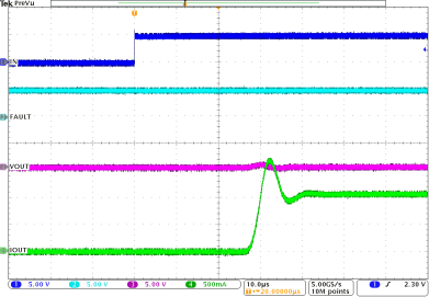
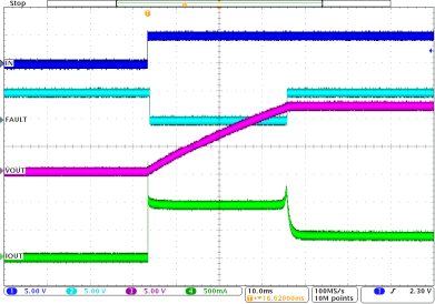
Figure 39 shows a test example of soft-start when driving a big capacitive load. Figure 40 shows an expanded waveform of the output current.
TPS2H160-Q1 app-curv1_SLVSD74.gif
VS = 12 V INx = ↑ Current limit = 1 A
Load current = 0.4 A CL = 2.3 mF CH1 = INx
CH2 = FAULT CH3 = output voltage CH4 = output current
Figure 39. Driving a Capacitive Load
TPS2H160-Q1 app-curv2_SLVSD74.gif
VVS = 12 V INx = ↑ Current limit = 1 A
Load current = 0.4 A CL = 2.3 mF CH1 = INx
CH2 = FAULT CH3 = output voltage CH4 = output current
Figure 40. Driving a Capacitive Load, Expanded Waveform

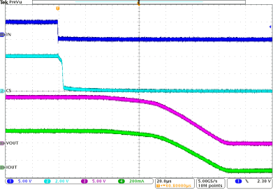
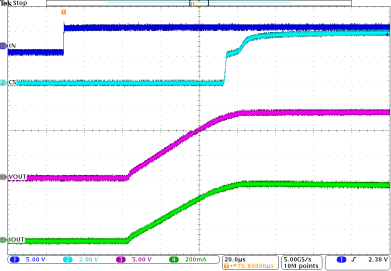
Figure 41 shows a test example of PWM-mode driving. Figure 42 shows the expanded waveform of the rising edge. Figure 43 shows the expanded waveform of the falling edge.
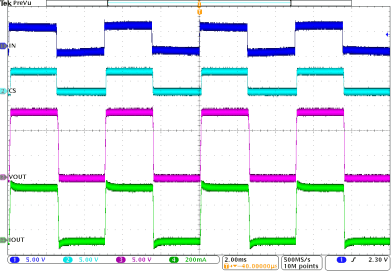
TPS2H160-Q1 app-curv3_SLVSD74.gif
VVS = 13.5 V INx = 200-Hz PWM at 50% duty cycle CH1 = INx signal
CH2 = CS voltage CH3 = output voltage CH4 = output current
Figure 41. PWM Signal Driving
TPS2H160-Q1 app-curv5_SLVSD74.gif
VVS = 13.5 V INx = 200-Hz PWM at 50% duty cycle CH1 = INx signal
CH2 = CS voltage CH3 = output voltage CH4 = output current
Figure 43. Expanded Waveform of Falling Edge
TPS2H160-Q1 app-curv4_SLVSD74.gif
VVS = 13.5 V INx = 200-Hz PWM at 50% duty cycle CH1 = INx signal
CH2 = CS voltage CH3 = output voltage CH4 = output current
Figure 42. Expanded Waveform of Rising Edge