SLVSA75A July 2010 – August 2015 TPS386596
PRODUCTION DATA.
- 1 Features
- 2 Applications
- 3 Description
- 4 Revision History
- 5 Pin Configuration and Functions
- 6 Specifications
- 7 Parameter Measurement Information
- 8 Detailed Description
- 9 Application and Implementation
- 10Power Supply Recommendations
- 11Layout
- 12Device and Documentation Support
- 13Mechanical, Packaging, and Orderable Information
8 Detailed Description
8.1 Overview
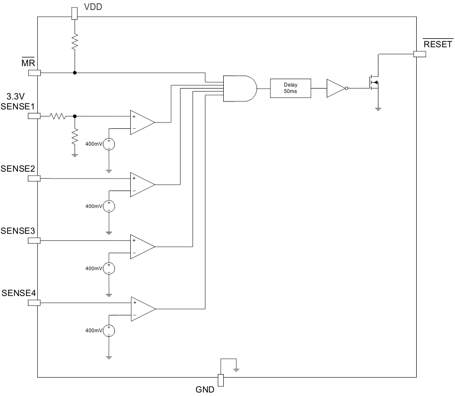
The TPS386596L33 multi-channel reset supervisor provides a complete single reset function for a four power supply system. The design of the SVS is based on the TPS386000 quad supervisor device series. The TPS386596 is designed to assert the RESET signal following the logic in Table 1. The RESET output remains asserted for a 50-ms delay time (td) after the event of reset release. The SENSE1 input has a fixed voltage threshold designed to monitor a 3.3-V nominal supply. The trip point, VIT1, for SENSE1 is 2.90 V (typical). Each of the remaining SENSEn inputs (n = 2, 3, 4) can be set to any voltage threshold greater than 0.4 V using an external resistor divider. An active-low manual reset (MR) input is also provided for asserting the RESET signal as desired by the system, regardless of the voltage on any of the SENSE pins.
8.3 Feature Description
8.3.1 Voltage Monitoring
Each SENSEn (n = 2, 3, 4) pin can be set to monitor any voltage threshold greater than 0.4 V using an external resistor divider. The SENSE1 pin is designed to monitor a 3.3-V supply with a 2.9-V threshold. A broad range of voltage thresholds can be supported, allowing these devices to be used in a wide array of applications.
The TPS386596 is relatively immune to short negative transients on the SENSEn pin. Sensitivity to transients depends on threshold overdrive, as shown in the typical performance graph TPS386596 SENSEn Minimum Pulse Width vs SENSEn Threshold Overdrive Voltage (Figure 4).
8.3.2 Manual Reset
The manual reset MR input allows external logic signal from processors, other logic circuits, and/or discrete sensors to initiate a reset. The typical application of a TPS386596 has its RESET output connected to processor. A logic low at MR causes RESET to assert. After MR returns to a logic high and SENSEn are above the respective voltage thresholds, RESET is released after a fixed 50-ms reset delay time. An internal 100-kΩ pullup to VDD is integrated on the MR input. There is also an internal 50-ns (typical) deglitch circuit.
8.3.3 Reset Output
In a typical application of the TPS386596, the RESET output is connected to the reset input of a processor (DSP, MCU, CPU, FPGA, ASIC, and so forth) or connected to the enable input of voltage regulators (DC-DC, LDO, and so forth).
The TPS386596 provides an open-drain reset output. Pullup resistors must be used to hold this line high when RESET is not asserted. By connecting a pullup resistor to the proper voltage rail (up to 6.5 V), the RESET output can be connected to other devices at the proper interface voltage level. The pullup resistor should be no smaller than 10 kΩ due to the finite impedance of the output transistor.
The RESET output is defined for VDD > 0.9 V. To ensure that the target processor is properly reset, the VDD supply input should be fed by the power rail and be available as early as possible in the application.
Table 1 shows a truth table of how the RESET output is asserted or released. Figure 1 provides a timing diagram that shows how RESET is asserted and deasserted in relation to MR and the SENSEn inputs. Once the conditions are met, the transitions from the asserted state to the release state are performed after a fixed 50-ms delay time.
8.4 Device Functional Modes
Table 1 shows the device functional modes.
Table 1. RESET Truth Table
| CONDITION | OUTPUT | ||
|---|---|---|---|
| MR = L | SENSEn < VITn | RESET = L | Reset asserted |
| MR = L | SENSEn > VITn | RESET = L | Reset asserted |
| MR = H | SENSE1 < VIT1 OR SENSE2 < VIT2 OR SENSE3 < VIT3 OR SENSE4 < VIT4 |
RESET = L | Reset asserted |
| MR = H | SENSE1 > VIT1 AND SENSE2 > VIT2 AND SENSE3 > VIT3 AND SENSE4 > VIT4 |
RESET = H | Reset released |
