JAJSOH5D November 2022 – November 2023 TPS389C03-Q1
PRODUCTION DATA
- 1
- 1 特長
- 2 アプリケーション
- 3 概要
- 4 Device Comparison
- 5 Pin Configuration and Functions
- 6 Specifications
- 7 Detailed Description
- 8 Register Maps
- 9 Application and Implementation
- 10Device and Documentation Support
- 11Revision History
- 12Mechanical, Packaging, and Orderable Information
パッケージ・オプション
メカニカル・データ(パッケージ|ピン)
- RTE|16
サーマルパッド・メカニカル・データ
- RTE|16
発注情報
7.3.4 MON
The TPS389C03-Q1 combines two comparators with a precision reference voltage and a trimmed resistor divider per monitor (MON) channel. This configuration optimizes device accuracy because all resistor tolerances are accounted for in the accuracy and performance specifications. Both comparators also include built-in hysteresis that provides noise immunity and provides stable operation.
Each MON channel can be configured for Low Frequency (LF) and High Frequency (HF) fault detection. HF fault detection uses a comparator for UV and OV measurements referenced to the threshold voltage. A debounce filter for glitch immunity can be configured for HF faults using the FLT_HF registers in BANK1 associated with each MON channel.
LF fault detection measures the voltage through an ADC that can be used to monitor voltage drift. The LF detection thresholds can be configured for various purposes. For example, the OVLF threshold can be set lower than the OVHF threshold for drift monitoring. Alternatively, the OVLF threshold can be set to overlap with the OVHF threshold for redundancy. LF and HF faults are configured using the UV_HF, OV_HF, UV_LF, and OV_LF registers in BANK1. Each MON channel has unique UV_HF, OV_HF, UV_LF, and OV_LF registers. The diagram shown in Figure 7-6 illustrates an example of how the LF and HF faults can be configured.
 Figure 7-6 MON Channel State Diagram
Although not required in most cases, for noisy applications good analog design practice is to place a 1-nF to 10-nF bypass capacitor at the MON input to reduce sensitivity to transient voltages on the monitored signal. Specific debounce times or deglitch times can also be set independently for each MON via I2C registers
When monitoring VDD supply voltage, the MON pin can be connected directly to VDD. The outputs NIRQ and NRST are high impedance when voltage at the MON pin is between upper and lower boundary of threshold.
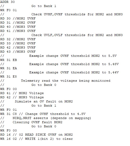
The MON channel settings can be adjusted by using the associated registers listed in the register maps found in Section 8. Using the register maps, the code example in Figure 7-15 demonstrates how MON2 can be reconfigured.
 Figure 7-7 MON2 Setting Software
Example