JAJSR60F August 2008 – June 2020 TPS40210-Q1 , TPS40211-Q1
PRODUCTION DATA
- 1
- 1 特長
- 2 アプリケーション
- 3 概要
- 5
- 4 Revision History
- 5 Pin Configuration and Functions
- 6 Specifications
-
7 Detailed Description
- 7.1 Overview
- 7.2 Functional Block Diagram
- 7.3
Feature Description
- 7.3.1 Minimum On-Time and Off-Time Considerations
- 7.3.2 Current Sense and Overcurrent
- 7.3.3 Current Sense and Subharmonic Instability
- 7.3.4 Current Sense Filtering
- 7.3.5 Soft Start
- 7.3.6 BP Regulator
- 7.3.7 Shutdown (DIS/ EN Pin)
- 7.3.8 Control Loop Considerations
- 7.3.9 Gate Drive Circuit
- 7.3.10 TPS40211-Q1
- 7.4 Device Functional Modes
-
8 Application and Implementation
- 8.1 Application Information
- 8.2
Typical Application
- 8.2.1 Design Requirements
- 8.2.2
Detailed Design Procedure
- 8.2.2.1 Duty Cycle Estimation
- 8.2.2.2 Inductor Selection
- 8.2.2.3 Rectifier Diode Selection
- 8.2.2.4 Output Capacitor Selection
- 8.2.2.5 Input Capacitor Selection
- 8.2.2.6 Current Sense and Current Limit
- 8.2.2.7 Current Sense Filter
- 8.2.2.8 Switching MOSFET Selection
- 8.2.2.9 Feedback Divider Resistors
- 8.2.2.10 Error Amplifier Compensation
- 8.2.2.11 R-C Oscillator
- 8.2.2.12 Soft-Start Capacitor
- 8.2.2.13 Regulator Bypass
- 8.2.3 Application Curves
- 9 Power Supply Recommendations
- 10Layout
- 11Device and Documentation Support
- 12Mechanical, Packaging, and Orderable Information
パッケージ・オプション
デバイスごとのパッケージ図は、PDF版データシートをご参照ください。
メカニカル・データ(パッケージ|ピン)
- DGQ|10
サーマルパッド・メカニカル・データ
発注情報
8.2.2.3 Rectifier Diode Selection
A low-forward voltage drop Schottky diode is used as a rectifier diode to reduce its power dissipation and improve efficiency. Using 80% derating, on VOUT for ringing on the switch node, the rectifier diode minimum reverse break-down voltage is given by Equation 41.
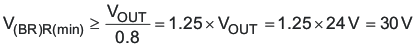
The diode must have reverse breakdown voltage greater than 30 V. The rectifier diode peak and average currents are estimated by Equation 42 and Equation 43.
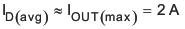
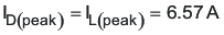
For this design, 2-A average and 6.57-A peak is:
The power dissipation in the diode is estimated by Equation 44.

For this design, the maximum power dissipation is estimated as 1 W. Reviewing 30-V and 40-V Schottky diodes, the MBRS340T3 40-V 3-A diode in an SMC package is selected. This diode has a forward voltage drop of 0.48 V at 6 A, so the conduction power dissipation is approximately 960 mW, less than half its rated power dissipation.