SLUS930D April 2011 – November 2016 TPS40400
PRODUCTION DATA.
- 1 Features
- 2 Applications
- 3 Description
- 4 Revision History
- 5 Pin Configuration and Functions
- 6 Specifications
-
7 Detailed Description
- 7.1 Overview
- 7.2 Functional Block Diagram
- 7.3
Feature Description
- 7.3.1 Output Voltage Setting
- 7.3.2 Input Voltage Feedforward
- 7.3.3 Output Current Limit and Warning
- 7.3.4 Linear Regulators
- 7.3.5 PMBus Address
- 7.3.6 PMBus Connections
- 7.3.7
PMBus Functionality and Additional Set-Up
- 7.3.7.1 Data Format
- 7.3.7.2 Output Voltage Adjustment
- 7.3.7.3 Overcurrent Threshold
- 7.3.7.4 Output Current Reading
- 7.3.7.5 Soft-Start Time
- 7.3.7.6 Power Good
- 7.3.7.7 Undervoltage Lockout (UVLO)
- 7.3.7.8 Output Overvoltage and Undervoltage Thresholds
- 7.3.7.9 Programmable Fault Responses
- 7.3.7.10 User Data and Adjustable Anti-Cross-Conduction Delay
- 7.4 Device Functional Modes
- 7.5 Programming
- 7.6
Register Maps
- 7.6.1 OPERATION (01h)
- 7.6.2 ON_OFF_CONFIG (02h)
- 7.6.3 CLEAR_FAULTS (03h)
- 7.6.4 WRITE_PROTECT (10h)
- 7.6.5 STORE_DEFAULT_ALL (11h)
- 7.6.6 RESTORE_DEFAULT_ALL (12h)
- 7.6.7 STORE_DEFAULT_CODE (13h)
- 7.6.8 RESTORE_DEFAULT_CODE (14h)
- 7.6.9 VOUT_MODE (20h)
- 7.6.10 VOUT_TRIM (22h)
- 7.6.11 VOUT_MARGIN_HIGH (25h)
- 7.6.12 VOUT_MARGIN_LOW (26h)
- 7.6.13 VOUT_SCALE_LOOP (29h)
- 7.6.14 FREQUENCY_SWITCH (33h)
- 7.6.15 VIN_ON (35h)
- 7.6.16 VIN_OFF (36h)
- 7.6.17 IOUT_CAL_GAIN (38h)
- 7.6.18 IOUT_CAL_OFFSET (39h)
- 7.6.19 VOUT_OV_FAULT_LIMIT (40h)
- 7.6.20 VOUT_OV_FAULT_RESPONSE (41h)
- 7.6.21 VOUT_UV_FAULT_LIMIT (44h)
- 7.6.22 VOUT_UV_FAULT_RESPONSE (45h)
- 7.6.23 IOUT_OC_FAULT_LIMIT (46h)
- 7.6.24 IOUT_OC_FAULT_RESPONSE (47h)
- 7.6.25 IOUT_OC_WARN_LIMIT (4Ah)
- 7.6.26 OT_FAULT_RESPONSE (50h)
- 7.6.27 POWER_GOOD_ON (5Eh)
- 7.6.28 POWER_GOOD_OFF (5Fh)
- 7.6.29 TON_RISE (61h)
- 7.6.30 STATUS_BYTE (78h)
- 7.6.31 STATUS_WORD (78h)
- 7.6.32 STATUS_VOUT (7Ah)
- 7.6.33 STATUS_IOUT (7Bh)
- 7.6.34 STATUS_TEMPERATURE (7Dh)
- 7.6.35 STATUS_CML (7Eh)
- 7.6.36 READ_VIN (88h)
- 7.6.37 READ_VOUT (8Bh)
- 7.6.38 READ_IOUT (8Ch)
- 7.6.39 PMBUS_REVISION (98h)
- 7.6.40 MFR_VIN_MIN (A0h)
- 7.6.41 MFR_VIN_MAX (A1h)
- 7.6.42 MFR_VOUT_MIN (A4h)
- 7.6.43 MFR_VOUT_MAX (A5h)
- 7.6.44 MFR_SPECIFIC_00 (D0h)
- 7.6.45 MFR_SPECIFIC_01 (D1h)
- 7.6.46 MFR_SPECIFIC_02 (D2h)
- 7.6.47 MFR_SPECIFIC_03 (D3h)
- 7.6.48 MFR_SPECIFIC_04 (D4h)
- 7.6.49 MFR_SPECIFIC_05 (D5h)
- 7.6.50 MFR_SPECIFIC_06 (D6h)
- 7.6.51 MFR_SPECIFIC_07 (D7h)
- 7.6.52 MFR_SPECIFIC_44 (FCh)
-
8 Application and Implementation
- 8.1 Application Information
- 8.2
Typical Applications
- 8.2.1
TPS40400 12-V Input, 1.2-V Output, 20-A (maximum) Output Current ConverterAdded Design Example 1
- 8.2.1.1 Design Requirements
- 8.2.1.2
Detailed Design Procedure
- 8.2.1.2.1 Selecting a Switching Frequency
- 8.2.1.2.2 Output Inductor, LOUT
- 8.2.1.2.3 Output Capacitance, COUT
- 8.2.1.2.4 The Resistive Component of Output Ripple
- 8.2.1.2.5 Peak Current Rating of the Inductor
- 8.2.1.2.6 Input Capacitance, CIN
- 8.2.1.2.7 Switching MOSFETs, QHS and QLS
- 8.2.1.2.8 Device Addressing, RADDR0 and RADDR1
- 8.2.1.2.9 Current Sense Flter, R16 and C17
- 8.2.1.2.10 Voltage Decoupling Capacitors, CBP3, CBP6, and CVDD
- 8.2.1.2.11 Bootstrap Capacitor, C9
- 8.2.1.2.12 Snubber R12 and C16
- 8.2.1.2.13 Loop Compensaton Components
- 8.2.1.2.14 Output Voltage Set Point, RBIAS
- 8.2.1.2.15 Remote Sensing
- 8.2.1.3 Application Curves
- 8.2.2 TPS40400 12-V Input 5-V Output, 5-A (Maximum) Output Current Converter Design Example 2Added Design Example 2
- 8.2.1
TPS40400 12-V Input, 1.2-V Output, 20-A (maximum) Output Current ConverterAdded Design Example 1
- 8.3 Initialization Setup
- 9 Power Supply Recommendations
- 10Layout
- 11Device and Documentation Support
- 12Mechanical, Packaging, and Orderable Information
8 Application and Implementation
NOTE
Information in the following applications sections is not part of the TI component specification, and TI does not warrant its accuracy or completeness. TI’s customers are responsible for determining suitability of components for their purposes. Customers should validate and test their design implementation to confirm system functionality.
8.1 Application Information
The TPS40400 device is a step-down DC-DC controller with integrated MOSFET drivers. Input voltage, output voltage and output current telemetry, parametric configuration, and protection features are programmable via the PMBus interface. The device is typically paired with two power MOSFETs and an L-C filter output stage to convert a higher DC voltage to a lower DC voltage. The available output current of a converter using the TPS40400 controller is limited by the choice of power stage components, and over-current protection levels. The maximum allowable over-current protection threshold is 35 A. Use the following design procedure to select component values for a TPS40400 converter. A Loop Compensation Calculator tool is available at www.ti.com to calculate the control loop compensation components, required for stability. The TPS40400 is also supported by Texas Instruments Fusion Digital Power Designer, a graphical software tool set designed to simplify programming, monitoring and configuration of the TPS40400 device via the PMBus interface.
8.2 Typical Applications
8.2.1 TPS40400 12-V Input, 1.2-V Output, 20-A (maximum) Output Current Converter
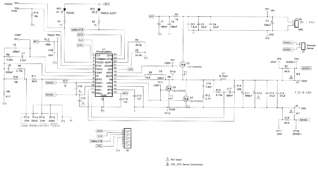 Figure 21. Typical Application Schematic, TPS40400
8.2.1.1 Design Requirements
The following example shows the design process and component selection for a synchronous buck converter using the TPS40400. The design goal parameters are listed in Table 62.
Table 62. Design Parameters
| PARAMETER | TEST CONDITIONS | MIN | NOM | MAX | UNIT | |
|---|---|---|---|---|---|---|
| INPUT CHARACTERISTICS | ||||||
| VIN | Input voltage | 8 | 12 | 14 | V | |
| IIN | Input current | VIN = 8 V, IOUT = 20 A | 3.6 | A | ||
| No load input current | VIN = 12 V, IOUT = 0 A | 60 | mA | |||
| VIN(start) | VIN start voltage | 7 | V | |||
| VIN(stop) | VIN stop voltage | 5 | V | |||
| OUTPUT CHARACTERISTICS | ||||||
| VOUT | Output voltage | VIN = 12 V, IOUT = 20 A | 1.08 | 1.2 | 1.32 | V |
| Line regulation | 8 ≤ VIN ≤ 14 V, IOUT = 20 A | 0.5% | ||||
| Load regulation | VIN = 12 V, 0 A ≤ IOUT ≤ 20 A | 0.5% | ||||
| Vout_ripple | Output ripple voltage | VIN = 12 V, IOUT = 20 A | 50 | mVP-P | ||
| Iout | Output current | 8 ≤ VIN ≤ 14 | 0 | 20 | A | |
| IOCP | Output over current inception point | VIN = 12 V | 21 | 25 | 29 | A |
| SS | Soft-start time | (default) | 2.8 | ms | ||
| Transient response | ||||||
| ΔI | Load step | 10 A ≤ IOUT ≤ 20 A | 10 | A | ||
| Load slew rate | 1 | A/μS | ||||
| Overshoot | 120 | mV | ||||
| Settling time | 20 | μs | ||||
| SYSTEM CHARACTERISTICS | ||||||
| fSW | Switching frequency | 300 | kHz | |||
| ηPK | Peak efficiency | VIN = 12 V, 0 A ≤ IOUT ≤ 20 A | 90% | |||
| η | Full load efficiency | VIN = 12 V, IOUT = 20 A | 85% | |||
| TOPER | Operating temperature range | 8 ≤ VIN ≤ 14 V, 0 A ≤ IOUT ≤ 20 A | –40 | 60 | °C | |
8.2.1.1.1 Design Example List of Materials
Table 63 lists of materials for the 12-V Input, 1.2-V Output, 20-A (maximum) Output Current Converter design.
Table 63. List of Materials
| REFERENCE DESIGNATOR | QTY | VALUE | DESCRIPTION | SIZE | PART NUMBER | MFR |
|---|---|---|---|---|---|---|
| C1, C2, C9, C17 | 4 | 100 nF | Ceramic, 25 V, X7R, 10% | 0603 | Std | Std |
| C11 | 1 | 680 µF | Tantalum, 6.3 V, 10% | 7343 (D) | TPSE687K006R0045 | AVX |
| C13, C14 | 2 | 47 µF | Ceramic, 6.3 V, X7R, 10% | 1210 | Std | Std |
| C15, C18 | 2 | 1 µF | Ceramic, 16 V, X7R, 10% | 0805 | Std | Std |
| C16 | 1 | 1.0 nF | Ceramic, 25 V, X7R, 10% | 0603 | Std | Std |
| C20 | 1 | 10 nF | Ceramic, 50 V, X7R, 10% | 0603 | Std | Std |
| C21 | 1 | 1.0 µF | Ceramic, 25 V, X7R, 10% | 1206 | Std | Std |
| C3, C4 | 2 | 22 µF | Ceramic, 25 V, X7R, 10% | 1210 | Std | Std |
| C5 | 1 | 330 µF | Aluminum, 25 V, 150 mΩ, FC series | 10 mm x 12 mm | EEVFC1E331P | Panasonic |
| C6 | 1 | 680 pF | Ceramic, 50 V, X7R, 10% | 0603 | Std | Std |
| C7 | 1 | 2.2 nF | Ceramic, 50 V, X7R, 10% | 0603 | Std | Std |
| C8 | 1 | 820 pF | Ceramic, 50 V, X7R, 10% | 0603 | Std | Std |
| D1, D2 | 2 | RED | LED, Red, 20-mA, 6-mcd | 0603 | LTST-C190CKT | Lite On |
| J1, J2 | 2 | D120/2DS | Terminal block, 2-pin, 15-A, 5.1mm | 0.40 inch x 0.35 inch | ED120/2DS | On Shore Technology |
| J3, J4 | 2 | L35 | Type L - copper single conductor, one-hole mount | 0.813 inch x 0.375 inch | L35 | Thomas and Betts |
| J6 | 1 | 86479-3 | Male right angle 2 x 5-pin, 100mil spacing | 0.607 inch x 0.484 inch | 86479-3 | AMP |
| JP1, JP2 | 2 | PEC02SAAN | Header, 2-pin, 100 mil Spacing | 0.100 inch x 2 | PEC02SAAN | Sullins |
| L1 | 1 | 0.75 µH | Inductor, SMT, 0.75 µH, 1.2 mΩ, 31A | 0.512 x 0.571 inch | PG0077.801 | Pulse |
| Q1 | 1 | CSD16404Q5A | MOSFET, N-channel, 25 V, 20 A, 4.1 mΩ | QFN5X6mm | CSD16404Q5A | TI |
| Q2, Q3 | 2 | CSD16325Q5 | MOSFET, N-channel, 25 V, 33 A, 1.7 mΩ | QFN-8 POWER | CSD16325Q5 | TI |
| R1, R2 | 2 | 1 kΩ | Resistor, 1/16-W, 5% | 0603 | Std | Std |
| R10, R17, R19 | 3 | 10 kΩ | Resistor, 1/16W, 1% | 0603 | Std | Std |
| R12 | 1 | 2.74 kΩ | Resistor, 1/8W, 1% | 1206 | Std | Std |
| R13 | 1 | 100 kΩ | Resistor, 1/16W, 1% | 0603 | Std | Std |
| R14 | 1 | 200 Ω | Resistor, 1/16W, 1% | 0603 | Std | Std |
| R15 | 1 | 0 Ω | Resistor, 1/16W, 1% | 0603 | Std | Std |
| R16 | 1 | 6.19 kΩ | Resistor, 1/16W, 1% | 0603 | Std | Std |
| R3, R9 | 2 | 10 Ω | Resistor, 1/16W, 1% | 0603 | Std | Std |
| R4 | 1 | 36.5 kΩ | Resistor, 1/16W, 1% | 0603 | Std | Std |
| R5 | 1 | 54.9 kΩ | Resistor, 1/16W, 1% | 0603 | Std | Std |
| R6 | 1 | 4.99 kΩ | Resistor, 1/16W, 1% | 0603 | Std | Std |
| R7, R11, R18 | 3 | 49.9 Ω | Resistor, 1/16W, 1% | 0603 | Std | Std |
| R8 | 1 | 2.74 kΩ | Resistor, 1/16W, 1% | 0603 | Std | Std |
| U1 | 1 | TPS40400RHL | 3.0 V to 20 V PMBus synchronous buck controller | QFN-24 | TPS40400RHL | TI |
8.2.1.2 Detailed Design Procedure
The following design example is for an output of 1.2 V at 20-A maximum, with an input range of 8 V to 14 V.
8.2.1.2.1 Selecting a Switching Frequency
This design example is calculated for a switching frequency of 300 kHz to improve efficiency. The switching frequency can be changed with the Fusion GUI, but some components may need to be revised at other switching frequencies.
8.2.1.2.2 Output Inductor, LOUT
The output inductor value is determined by the peak-to-peak ripple at high line, and in this case a value of 30% of output current maximum is used.

For this design a 750-nH inductor from Pulse (PG0077.801) was selected. The actual ripple current should now be recalculated using the actual inductance value.

With this ripple current, the inductor RMS and peak current values can be calculated.
The RMS value of a zero-average triangular wave is given by Equation 38.

At maximum load and maximum line, the peak inductor current is given by Equation 39.

The DCR of the selected inductor (from the data sheet) is 1.2 mΩ. Inductor conduction losses are described in Equation 40.

8.2.1.2.3 Output Capacitance, COUT
The selection of the output capacitor is typically affected by the output transient response requirement. Equation 41 and Equation 42 can be used to over-estimate the voltage deviation to account for delays in the loop bandwidth and can be used to determine the required output capacitance. The estimate of COUT based on overshoot is shown in Equation 41.

The estimate of COUT based on undershoot is shown in Equation 42.

When VIN(min) > 2 x VOUT, use the overshoot equation (VOvershoot) to calculate minimum output capacitance.
When VIN(min) < 2 x VOUT use the undershoot equation (VUndershoot). In this design example, VIN(min) is much larger than 2 x VOUT so Equation 43 is used to determine the required minimum output capacitance.

8.2.1.2.4 The Resistive Component of Output Ripple
With a minimum capacitance, the maximum allowable ESR is determined by the maximum ripple voltage and is approximated by Equation 44.

The factor of 8 in the equation above results from the calculation of capacitor voltage resulting from a triangular current. For this design, a 680-µF, 45-mΩ ESR, 5-nH ESL tantalum and two, 47-µF, 3-mΩ ESR, 0.9-nH ESL ceramic capacitors were selected for a total capacitance of 780 µF.
8.2.1.2.5 Peak Current Rating of the Inductor
With the output capacitance known, it is possible to calculate the charge current during start-up and determine the minimum saturation current rating for the inductor. The start-up charging current is shown in Equation 45 and the resulting peak inductor current is shown in Equation 46 .


8.2.1.2.6 Input Capacitance, CIN
The input capacitor is selected to limit the input ripple voltage to 20% or less of VIN. The ripple voltage is due to the current flowing in the input capacitor’s ESR as well as capacitance charging and discharging. To simplify the calculations, an infinitely large series input inductance is assumed. With an infinite inductor, the input capacitor current is calculated to be 5.6 Arms.
For reasons of availability, consider the capacitor EEVFC1E331P, which is an electrolytic, 330-µF, 25-V capacitor with 150-mΩ of ESR and 100-nH ESL. This capacitor has an rms current rating of 670 mA. With the calculated rms value of the capacitor current of 5.6 Arms, this implies that needs to be additional capacitance with a much lower ESR across the input bus in order to divert most of the AC current to this low ESR capacitor.
Another readily available capacitor is selected. A 22-µF, ceramic, 25-V, 10-mΩ ESR, 0.9-nH ESL device, two in parallel. With these capacitors in parallel, the ripple in the electrolytic is well within its rating with a value of 329 mArms.
8.2.1.2.7 Switching MOSFETs, QHS and QLS
The high-side and low-side MOSFETs, QHS and QLS, are selected based on several factors including:
- Vds, the drain to source voltage rating. This design requires a 25-V device
- Vgs, the gate to source voltage rating. For the TPS40400 device this voltage is 6.5 V
- Conduction losses, based on I2×RDS(on)
- Gate charge, must be low enough to be driven by the PWM controller
These devices are selected:
Table 64. MOSFET Summary
| LOCATION | PART NUMBER | VOLTAGE RATING (V) | RDS(on)
(mΩ) |
GATE CHARGE QG(nC) |
QTY |
|---|---|---|---|---|---|
| High-side | CSD16404Q5A | 25 | 4.1 | 8 | 1 |
| Low-side | CSD16325Q5 | 25 | 1.7 | 25 | 2 |
Because the selected MOSFETs are switch very quickly, the device is programmed to have the shorter dead-time of 25 ns.
8.2.1.2.8 Device Addressing, RADDR0 and RADDR1
The PMBus address for the device must be read from the ADDR0 and ADDR1 pins. Each pin has an internal fixed current source and the resulting developed voltage is read and converted to the desired device address. The external resistors RADDR0 and RADDR1 from the address pins to ground set eight possible states for a total of 64 possible addresses. The address states are determined by voltages on the address pins per Table 65.
Table 65. Address Configuration
| DIGIT | RESISTANCE (kΩ) |
|---|---|
| 0 | 10 |
| 1 | 15.4 |
| 2 | 23.7 |
| 3 | 36.5 |
| 4 | 54.9 |
| 5 | 84.5 |
| 6 | 130 |
| 7 | 200 |
For this design, the address of 34 octal, or 28 decimal is selected arbitrarily. In order to achieve this address, the ADDR0 resistor R5 would be 54.9 kΩ and the ADDR1 resistor R4 would be 36.5 kΩ.
8.2.1.2.9 Current Sense Flter, R16 and C17
Current sensing for the TPS40400 device is typically done by sensing the voltage drop across the output inductor’s (L1) DC resistance. In order to do this, the large AC switching voltage forced across L1 must be filtered out so that the measured voltage is only the DC drop. This is done by placing an R-C filter directly across the output choke (high-frequency filter) L1. The R-C combination is chosen such that it provides enough filtering for the application and the time constant is chosen to match that of the output inductor and its ESR, which is shown in Equation 47.

Usually a capacitor value is chosen between 10 nF and 1 µF for this location. A value of 100 nF is arbitrarily chosen, which yields Equation 48.

Choose a standard value of 6.19 kΩ.
The capacitor C17 should be placed as close to the ISNS+ and ISNS– pins as possible to provide good bypass filtering. R16 should be placed close to the inductor to prevent traces with the switch node voltage from being propagated across the PCB and getting close to sensitive pins of the TPS40400 device.
8.2.1.2.10 Voltage Decoupling Capacitors, CBP3, CBP6, and CVDD
Three pins on the TPS40400 device have DC bias voltages. It is necessary to add small decoupling capacitors to these pins. Table 66 shows the recommended minimum values.
Table 66. Voltage Decoupling Capacitor Values
| DEVICE LOCATION | RECOMMENDED MINIMUM VALUE | FUNCTION | SELECTED VALUE |
|---|---|---|---|
| CBP3, (C18) | 0.1-µF low ESR | VCC for internal controls of the device | 1-µF ceramic |
| CBP6, (C15) | 1-µF low ESR | VCC for gate drivers | 1-µF ceramic |
| CVDD, (C1) and (C2) | 0.1-µF low ESR | VCC for input power to the device | 2 x 100 nF, with additional series 10-Ω filter resistor R3 to filter out switching noise from the power MOSFETs |
8.2.1.2.11 Bootstrap Capacitor, C9
Selection of the bootstrap capacitor is based on the total gate charge of the high-side MOSFET and the allowable ripple on the BOOT pin. A ripple of 0.2 V is chosen as maximum for this design. This yields a value described in Equation 49.

Choose a standard value of 100 nF. Additionally, a series resistor R9 is added in order to reducing the turn-on speed of the high-side MOSFET, Q1.
8.2.1.2.12 Snubber R12 and C16
For this design, the snubber function is designed based on an allowable snubber power dissipation. A target value of between 0.25% and 0.5% of the rated output power (POUT) is used as the starting point for the calculation of the snubber values. Once the snubber values are determined and real hardware is obtained, the snubber values can be adjusted to achieve better results.


8.2.1.2.13 Loop Compensaton Components
Using the Texas Instruments SwitcherPro™ design tool and the resulting plant (system) bode plot, a crossover frequency of 20 kHz is selected with 45° of phase margin. The resulting compensation components are listed in Table 67.
Table 67. Component Summary
| COMPONENT LOCATION | VALUE |
|---|---|
| R6 | 4.99 kΩ |
| R8 | 2.74 kΩ |
| C6 | 680 pF |
| C7 | 2.2 nF |
| C8 | 820 pF |
8.2.1.2.14 Output Voltage Set Point, RBIAS
The output voltage can be set by choosing and calculating R1 and RBIAS. The VOUT set point is shown in Equation 53.

In this design R1 was chosen to be 10 kΩ. RBIAS is calculated to be 10 kΩ.
8.2.1.2.15 Remote Sensing
Remote sensing can be accomplished with the differential amplifier as shown in Figure 22. Resistors RS1 and RS2 (R7 and R18 in the schematic above) are used if the sense connections fail or get damaged. The values of RS1 and RS2 are bound by an upper value such that the voltage drop across them does not introduce appreciable voltage regulation error from the bias current, and a lower value such that the voltage drop in the load wires which appears across these resistors does not dissipate appreciable power. Values between 10 Ω to 50 Ω are usually chosen.
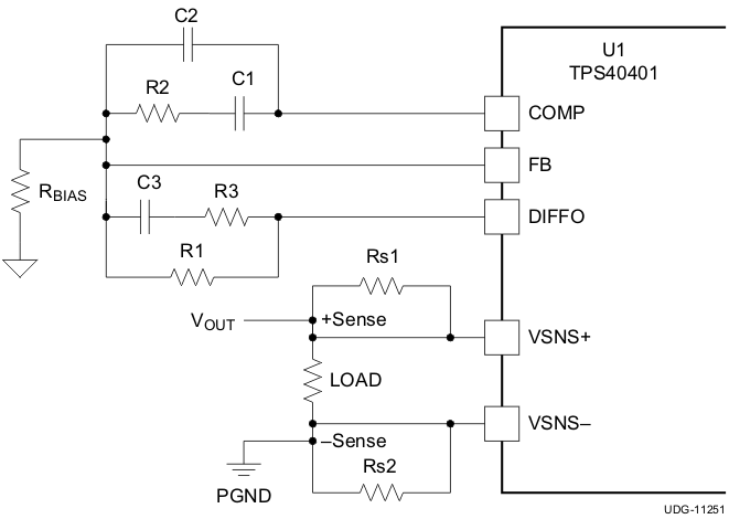 Figure 22. Remote Sense Function
8.2.1.3 Application Curves
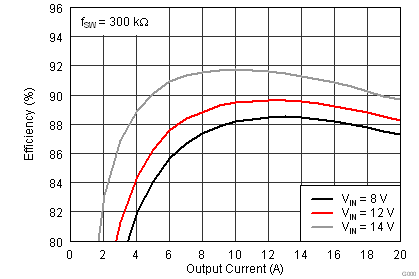 Figure 23. Efficiency
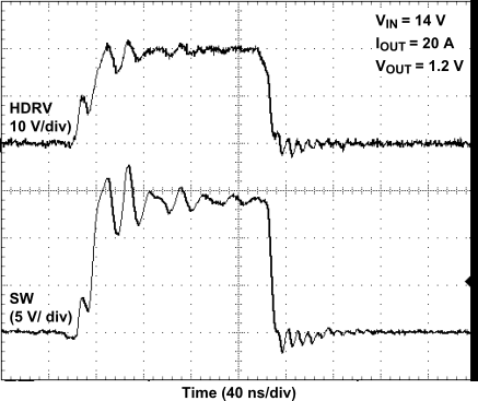 Figure 25. Switching Waveform
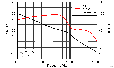 Figure 24. Plant (System) Bode
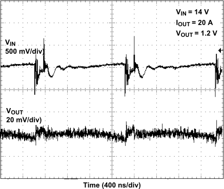 Figure 26. Ripple Waveform
8.2.2 TPS40400 12-V Input 5-V Output, 5-A (Maximum) Output Current Converter Design Example 2
 Figure 27. Typical Application Schematic, TPS40400 Design Example 2
8.2.2.1 Design Requirements
Figure 27 shiws the design process and component selection for a synchronous buck converter using the TPS40400 device. The design goal parameters are listed in Table 68.
Table 68. Electrical Parameters
| PARAMETER | TEST CONDITIONS | MIN | NOM | MAX | UNIT | |
|---|---|---|---|---|---|---|
| INPUT CHARACTERISTICS | ||||||
| VIN | Input voltage | 8 | 12 | 14 | V | |
| IIN | Input current | VIN = 8 V, IOUT = 5 A | 3.5 | A | ||
| No load input current | VIN = 12 V, IOUT = 0 A | 60 | mA | |||
| VIN(start) | VIN start voltage | 7 | V | |||
| VIN(stop) | VIN stop voltage | 6 | V | |||
| OUTPUT CHARACTERISTICS | ||||||
| VOUT | Output voltage | VIN = 12 V, IOUT = 5 A | 4.75 | 5 | 5.25 | V |
| Line regulation | 8 ≤ VIN ≤,14 V, IOUT = 5 A | 0.5% | ||||
| Load regulation | VIN = 12 V, 0 A ≤ IOUT ≤ 5 A | 0.5% | ||||
| VOUT(ripple) | Output ripple voltage | VIN = 12 V, IOUT = 5 A | 50 | mVP-P | ||
| Iout | Output current | 8 ≤ VIN ≤ 14 | 0 | 5 | A | |
| IOCP | Output over current inception point | VIN = 12 V | 6.7 | 8 | 9.3 | A |
| SS | Soft-start time | (default) | 5 | ms | ||
| Transient response | ||||||
| ΔI | Load step | 2 A ≤ IOUT ≤ 5 A | 3 | A | ||
| Load slew rate | 1 | A/μS | ||||
| Overshoot | 500 | mV | ||||
| Settling time | 50 | μs | ||||
| SYSTEM CHARACTERISTICS | ||||||
| fSW | Switching frequency | 300 | kHz | |||
| ηPK | Peak efficiency | VIN = 12 V, 0 A ≤ IOUT ≤ 5 A | 90% | |||
| η | Full load efficiency | VIN = 12 V, IOUT = 5 A | 85% | |||
| TOPER | Operating temperature range | 8 ≤ VIN ≤ 14 V, 0 A ≤ IOUT ≤ 5 A | –40 | 60 | °C | |
8.2.2.1.1 List of Materials
Table 69 lists the materials for Design Example 2.
Table 69. List of Materials
| REFERENCE DESIGNATOR | QTY | VALUE | DESCRIPTION | SIZE | PART NUMBER | MFR |
|---|---|---|---|---|---|---|
| C1, C2, C9, C17 | 4 | 0.1 µF | Ceramic, X7R, 25 V, 20% | 0603 | Standard | Standard |
| C3, C4 | 2 | 22 µF | Ceramic, X7R, 25 V, 10% | 1210 | Standard | Standard |
| C5 | 1 | 330 µF | Aluminum, 25 V, 20% | 10x12mm | EEVFC1E331P | Panasonic |
| C6 | 1 | 2700 pF | Ceramic, X7R, 10 V, 20% | 0603 | Standard | Standard |
| C7 | 1 | 470 pF | Ceramic, X7R, 10 V, 20% | 0603 | Standard | Standard |
| C8 | 1 | 2700 pF | Ceramic, X7R, 10 V, 20% | 0603 | Standard | Standard |
| C11 | 1 | 680 µF | Tantalum, 6.3 V, 20% | 7343 (D) | TPSE6870060045 | Standard |
| C13, C14 | 2 | 47 µF | Ceramic, X7R, 6.3 V, 20% | 1210 | GRM32ER60J476M | Standard |
| C15, C18 | 2 | 1 µF | Ceramic, X7R, 16 V, 20% | 0603 | Standard | Standard |
| C16 | 1 | 1000 pF | Ceramic, X7R, 25 V, 20% | 0603 | Standard | Standard |
| L1 | 1 | 6.8 µH | Inductor, 6.8 µH, 12 mΩ | PF0553.682NL | Pulse | |
| Q1 | 1 | CSD16325Q5 | Transistor, N-channel MOSFET, 25 V, 100 A, 10 Ω | QFN 5x6 | CSD16325Q5 | TI |
| Q2 | 1 | CSD16325Q5 | Transistor, N-channel, 25 V, 100 A, 10 Ω | QFN 5x6 | CSD16325Q5 | TI |
| R3 | 1 | 10 Ω | Resistor, 1/16W, 5% | 0603 | Standard | Standard |
| R4 | 1 | 39.2 kΩ | Resistor, 1/16W, 1% | 0603 | Standard | Standard |
| R5 | 1 | 64.9 kΩ | Resistor, 1/16W, 1% | 0603 | Standard | Standard |
| R6 | 1 | 10.7 kΩ | Resistor, 1/16W, 1% | 0603 | Standard | Standard |
| R7, R18 | 2 | 49.9 Ω | Resistor, 1/16W, 1% | 0603 | Standard | Standard |
| R8 | 1 | 1.62 kΩ | Resistor, 1/16W, 1% | 0603 | Standard | Standard |
| R10 | 1 | 10 kΩ | Resistor, 1/16W, 1% | 0603 | Standard | Standard |
| R12 | 1 | 2.7 Ω | Resistor, 1/16W, 5% | 0603 | Standard | Standard |
| R14 | 1 | 0.0 Ω | Resistor, 1/16W, 1% | 0603 | Standard | Standard |
| R16 | 1 | 5.71 kΩ | Resistor, 1/16W, 1% | 0603 | Standard | Standard |
| R17 | 1 | 1.33 kΩ | Resistor, 1/16W, 1% | 0603 | Standard | Standard |
| U1 | 1 | TPS40400 | 3.0V-20V PMBus synchronous buck controller | 24-pin QFN | TPS40400RHL | Texas Instruments |
8.2.2.2 Application Curves
 Figure 28. Switching Voltage and Inductor Current Waveform
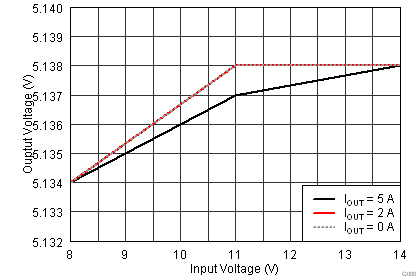 Figure 30. Line Regulation
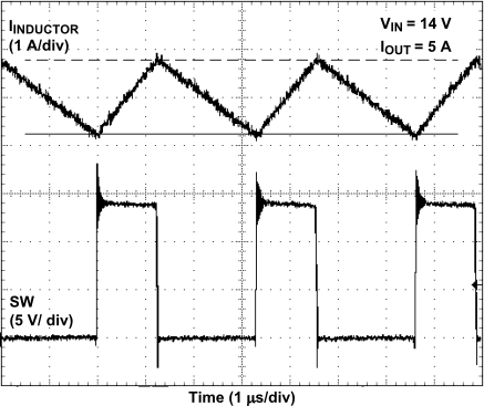 Figure 29. Switching Voltage and Inductor Current Waveform
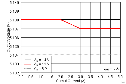 Figure 31. Load Regulation
8.3 Initialization Setup
8.3.1 Internal Configuration
Internal configuration of the TPS40400 device is handled via the PMBus (pins CLK and DATA) and the Fusion Digital Power Designer (GUI interface). An example of the configuration window that is used to make internal configuration changes to the TPS40400 device is shown below in Figure 32.
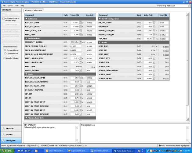 Figure 32. All Configuration Window
Figure 32 shows are the user changeable parameters of the TPS40400 device and these consist of the following sections.
- Calibration
- Configuration
- Limits
- On/Off Configuration
The status section is read only, and consists of data read from the TPS40400 device such as VOUT, IOUT, VIN, and status words. A full description of each command and status word is available in the Register Maps section.
Configuration changes can be implemented by changing the value in the Value/Edit box of each parameter. Most boxes allow direct parameter changes such as voltage or current, but some boxes such as IOUT_OC_FAULT_RESPONSE provide a pop-up configuration window as shown in Figure 33, and others provide a pull-down menu. Select the appropriate radio buttons to make the desired changes.
To implement the changes to the device, click on the [Write to Hardware] button. This stores the changes to the device in volatile memory, so these changes are lost when input power is cycled. To permanently make changes and commit those changes to non-volatile memory, click on the [Store RAM to Flash] button.
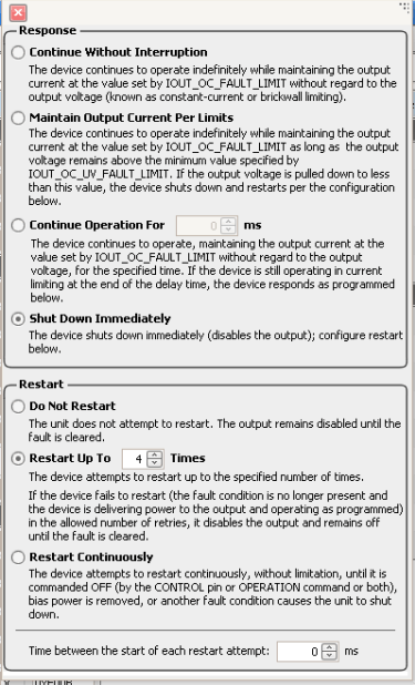 Figure 33. IOUT_OC_FAULT_RESPONSE Configuration Window