JAJSHA3K December 2012 – May 2019 TPS50301-HT
PRODUCTION DATA.
- 1 特長
- 2 アプリケーション
- 3 概要
- 4 改訂履歴
- 5 概要(続き)
- 6 Pin Configuration and Functions
- 7 Specifications
-
8 Detailed Description
- 8.1 Overview
- 8.2 Functional Block Diagram
- 8.3
Feature Description
- 8.3.1 VIN and Power VIN Pins (VIN and PVIN)
- 8.3.2 PVIN vs Frequency
- 8.3.3 Voltage Reference
- 8.3.4 Adjusting the Output Voltage
- 8.3.5 Maximum Duty Cycle Limit
- 8.3.6 PVIN vs Frequency
- 8.3.7 Safe Start-Up into Prebiased Outputs
- 8.3.8 Error Amplifier
- 8.3.9 Slope Compensation
- 8.3.10 Enable and Adjust UVLO
- 8.3.11 Adjustable Switching Frequency and Synchronization (SYNC)
- 8.3.12 Slow Start (SS/TR)
- 8.3.13 Power Good (PWRGD)
- 8.3.14 Bootstrap Voltage (BOOT) and Low Dropout Operation
- 8.3.15 Sequencing (SS/TR)
- 8.3.16 Output Overvoltage Protection (OVP)
- 8.3.17 Overcurrent Protection
- 8.3.18 TPS50301-HT Thermal Shutdown
- 8.3.19 Turn-On Behavior
- 8.3.20 Small Signal Model for Loop Response
- 8.3.21 Simple Small Signal Model for Peak Current Mode Control
- 8.3.22 Small Signal Model for Frequency Compensation
- 8.4 Device Functional Modes
-
9 Application and Implementation
- 9.1 Application Information
- 9.2
Typical Application
- 9.2.1 Design Requirements
- 9.2.2
Detailed Design Procedure
- 9.2.2.1 Custom Design With WEBENCH® Tools
- 9.2.2.2 Operating Frequency
- 9.2.2.3 Output Inductor Selection
- 9.2.2.4 Output Capacitor Selection
- 9.2.2.5 Input Capacitor Selection
- 9.2.2.6 Slow Start Capacitor Selection
- 9.2.2.7 Bootstrap Capacitor Selection
- 9.2.2.8 Undervoltage Lockout (UVLO) Set Point
- 9.2.2.9 Output Voltage Feedback Resistor Selection
- 9.2.2.10 Compensation Component Selection
- 9.2.3 Parallel Operation
- 9.2.4 Application Curve
- 10Power Supply Recommendations
- 11Layout
- 12デバイスおよびドキュメントのサポート
- 13メカニカル、パッケージ、および注文情報
9.2.3 Parallel Operation
Configuring two TPS50601-SP in order to provide 12-A output current.
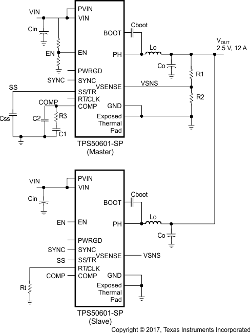
Design procedure is as follows - An example, Figure 30, shows parallel configuration using two TPS50601-SP in Master/Slave.
Important design steps are detailed as follows:
 Figure 30. Parallel Configuration Showing Master and Slave
 For the master - RT pin must be left floating and this will set the frequency to 500 kHz.
In order to parallel two current mode control POLs (TPS50601-SP) one needs to do the following:
- RT pin on master must be left open (switching frequency 500-kHz typical (395-kHz minimum to 585-kHz maximum)) as highlighted in the data sheet frequency internally generated. For more details, see Adjustable Switching Frequency and Synchronization (SYNC) section.
- When RT pin is left open then sync pin becomes output.
- RT pin on slave should be selected within 5% of master ie RT = 96-kHz typical.
- Have a single feedback loop.
- Sync pins of master must be connected to sync pins of slave.
- Connect comp pins of two POLs together.
- Connect Vsense pins of two POLs together.
- Connect SS pins together.
- Connect enable pins together thus there is one enable.
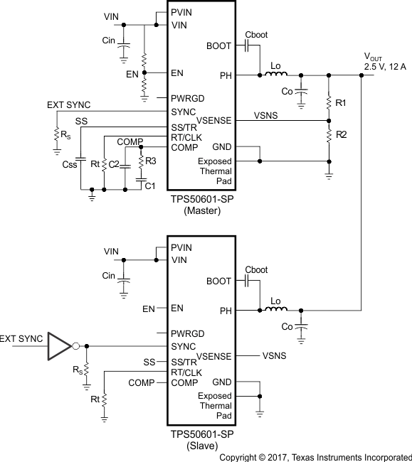
 Figure 31. Parallel Configuration With External Sync
 Configuration when using an external clock is as follows: Refer to Figure 31.
- Master/slave configuration can also be achieved if desired using external clock ie if operating at 100 kHZ or any other customer selected frequency.
- External user supplied clock signal is required.
- RT pins of both master and slave must be populated with appropriate resistor value ie 475 kΩ (for 100 kHZ).
- Slave signal feeding the sync pin must be inverter.
- RT pin on both master and slave must be populated for 100 kHz operation RT = 495 kΩ.
- External user supplied clock signal is required.
- Connect comp pins of two POLs together.
- Connect Vsense pins of two POLs together.
- Connect SS pins together.
- Connect enable pins together thus there is one enable.