JAJSJP3A September 2020 – October 2020 TPS51397A
PRODUCTION DATA
- 1 特長
- 2 アプリケーション
- 3 概要
- 4 Revision History
- 5 Pin Configuration and Functions
- 6 Specifications
- 7 Detailed Description
- 8 Application and Implementation
- 9 Power Supply Recommendations
- 10Layout
- 11Device and Documentation Support
- 12Mechanical, Packaging, and Orderable Information
7.3.1 PWM Operation and DCAP3 Control
The main control loop of the buck is an adaptive on-time pulse width modulation (PWM) controller that supports a proprietary DCAP3™ mode control. The DCAP3™ mode control combines adaptive on-time control with an internal compensation circuit for pseudo-fixed frequency and low external component count configuration with both low-ESR and ceramic output capacitors. It is stable even with virtually no ripple at the output. The TPS51397A also includes an error amplifier that makes the output voltage high accurate.
At the beginning of each cycle, the high-side MOSFET is turned on. This MOSFET is turned off after an internal one-shot timer expires. This one-shot duration is set proportional to the converter input voltage, VIN, and is inversely proportional to the output voltage, VOUT, to maintain a pseudo-fixed frequency over the input voltage range, hence it is called adaptive on-time control. The one-shot timer is reset and the high-side MOSFET is turned on again when the feedback voltage falls below the reference voltage. An internal ripple generation circuit is added to the reference voltage to emulate the output ripple. This enables the use of very low-ESR output capacitors such as multi-layered ceramic caps (MLCC). No external current sense network or loop compensation is required for DCAP3™ control topology.
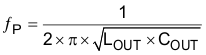
For any control topology that is compensated internally, there is a range of the output filter it can support. The output filter used with the TPS51397A is a low-pass L-C circuit. This L-C filter has a double-pole frequency described in Equation 1.
At low frequencies, the overall loop gain is set by the external output set-point resistor divider network and the internal gain of the TPS51397A. The low-frequency L-C double pole has a 180 degree lag in-phase. At the output filter frequency, the gain rolls off at a –40 dB per decade rate and the phase drops rapidly. The internal ripple generation network introduces a mid-frequency zero that reduces the gain roll off from –40 dB to –20 dB per decade and increases the phase to 90 degree one decade above the zero frequency. The inductor and capacitor selected for the output filter must be such that the double pole is placed close enough to the mid-frequency zero so that the phase boost provided by this mid-frequency zero provides adequate phase margin for the stability requirement. The crossover frequency of the overall system should usually be targeted to be less than one-third of the switching frequency (FSW).