SLUSC63A November 2015 – December 2015 TPS53317A
PRODUCTION DATA.
- 1 Features
- 2 Applications
- 3 Description
- 4 Revision History
- 5 Pin Configuration and Functions
- 6 Specifications
- 7 Detailed Description
- 8 Application and Implementation
- 9 Power Supply Recommendations
- 10Layout
- 11Device and Documentation Support
- 12Mechanical, Packaging, and Orderable Information
パッケージ・オプション
メカニカル・データ(パッケージ|ピン)
- RGB|20
サーマルパッド・メカニカル・データ
- RGB|20
発注情報
10 Layout
10.1 Layout Guidelines
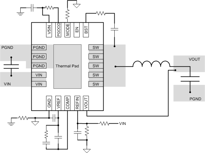
Stable power supply operation depends on proper layout. Follow these guidelines for an optimized PCB layout.
- Connect PGND pins to the thermal pad underneath the device. Use four vias to connect the thermal pad to internal ground planes.
- Place VIN, V5IN and VREF decoupling capacitors as close to the device as possible.
- Use wide traces for the VIN, PGND and SW pins. These nodes carry high current and also serve as heat sinks.
- Place feedback and compensation components as close to the device as possible.
- Place COMP and VOUT analog signal traces away from noisy signals (SW, BST).
- The GND pin should connect to the PGND in only one place, through a via or a 0-Ω resistor.
10.2 Layout Example
 Figure 42. TPS53317A Board Layout
10.3 Mounting and Thermal Profile Recommendation
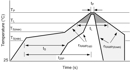
Proper mounting technique adequately covers the exposed thermal tab with solder. Excessive heat during the reflow process can affect electrical performance. Figure 43 shows the recommended reflow oven thermal profile. Proper post-assembly cleaning is also critical to device performance. See SLUA271 for more information.
 Figure 43. Recommended Reflow Oven Thermal Profile
Table 2. Recommended Thermal Profile Parameters
| PARAMETER | MIN | TYP | MAX | UNIT | |
|---|---|---|---|---|---|
| RAMP UP AND RAMP DOWN | |||||
| rRAMP(up) | Average ramp-up rate, TS(max) to TP | 3 | °C/s | ||
| rRAMP(down) | Average ramp-down rate, TP to TS(max) | 6 | °C/s | ||
| PRE-HEAT | |||||
| TS | Pre-Heat temperature | 150 | 200 | °C | |
| tS | Pre-heat time, TS(min) to TS(max) | 60 | 180 | s | |
| REFLOW | |||||
| TL | Liquidus temperature | 217 | °C | ||
| TP | Peak temperature | 260 | °C | ||
| tL | Time maintained above liquidus temperature, TL | 60 | 150 | s | |
| tP | Time maintained within 5 °C of peak temperature, TP | 20 | 40 | s | |
| t25P | Total time from 25 °C to peak temperature, TP | 480 | s | ||