JAJSBU2G August 2011 – April 2021 TPS53355
PRODUCTION DATA
- 1 特長
- 2 アプリケーション
- 3 概要
- 4 Revision History
- 5 Pin Configuration and Functions
- 6 Specifications
-
7 Detailed Description
- 7.1 Overview
- 7.2 Functional Block Diagram
- 7.3
Feature Description
- 7.3.1 5-V LDO and VREG Start-Up
- 7.3.2 Adaptive On-Time D-CAP Control and Frequency Selection
- 7.3.3 Ramp Signal
- 7.3.4 Adaptive Zero Crossing
- 7.3.5 Power-Good
- 7.3.6 Current Sense, Overcurrent and Short Circuit Protection
- 7.3.7 Overvoltage and Undervoltage Protection
- 7.3.8 UVLO Protection
- 7.3.9 Thermal Shutdown
- 7.4 Device Functional Modes
- 8 Application and Implementation
- 9 Power Supply Recommendations
- 10Layout
- 11Device and Documentation Support
- 12Mechanical, Packaging, and Orderable Information
パッケージ・オプション
デバイスごとのパッケージ図は、PDF版データシートをご参照ください。
メカニカル・データ(パッケージ|ピン)
- DQP|22
サーマルパッド・メカニカル・データ
- DQP|22
発注情報
7.4.2 Auto-Skip Eco-mode™ Light Load Operation
While the MODE pin is pulled low via RMODE, TPS53355 automatically reduces the switching frequency at light load conditions to maintain high efficiency. Detailed operation is described as follows. As the output current decreases from heavy load condition, the inductor current is also reduced and eventually comes to the point that its rippled valley touches zero level, which is the boundary between continuous conduction and discontinuous conduction modes. The synchronous MOSFET is turned off when this zero inductor current is detected. As the load current further decreases, the converter runs into discontinuous conduction mode (DCM). The on-time is kept almost the same as it was in the continuous conduction mode so that it takes longer time to discharge the output capacitor with smaller load current to the level of the reference voltage. The transition point to the light-load operation IOUT(LL) (i.e., the threshold between continuous and discontinuous conduction mode) can be calculated as shown in Equation 5.
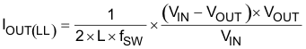
where
- ƒSW is the PWM switching frequency
Switching frequency versus output current in the light load condition is a function of L, VIN and VOUT, but it decreases almost proportionally to the output current from the IOUT(LL) given in Equation 5. For example, it is 60 kHz at IOUT(LL)/5 if the frequency setting is 300 kHz.