JAJSML7B March 2013 – August 2021 TPS53511
PRODUCTION DATA
- 1 特長
- 2 アプリケーション
- 3 概要
- 4 Revision History
- 5 Pin Configuration and Functions
- 6 Specifications
- 7 Detailed Description
- 8 Application and Implementation
- 9 Power Supply Recommendations
- 10Layout
- 11Device and Documentation Support
- 12Mechanical, Packaging, and Orderable Information
パッケージ・オプション
メカニカル・データ(パッケージ|ピン)
- RGT|16
サーマルパッド・メカニカル・データ
- RGT|16
発注情報
7.3.3 Soft Start and Pre-Biased Soft-Start Function
The soft-start time function is adjustable. When the EN pin becomes high, 2-µA current begins charging the capacitor, which is connected from the SS pin to GND. Smooth control of the output voltage is maintained during start up. The equation for the slow-start time is shown in Equation 1. The VFB voltage is 0.765 V and SS pin source current is 2 µA.
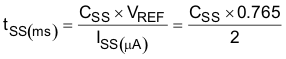
where
- CSS is the value of the capacitor connected between the SS pin and GND.
- CSS is expressed in nF.
This unique circuit prevents current from being pulled from the output during start-up if the output is pre-biased. When the soft start commands a voltage higher than the pre-bias level (internal soft-start voltage becomes greater than feedback voltage VFB), the controller slowly activates synchronous rectification by starting the first low-side FET gate driver pulses with a narrow on time. It then increments the on time on a cycle-by-cycle basis until it coincides with the time dictated by (1–D), where D is the duty cycle of the converter. This scheme prevents the initial sinking of the pre-bias output, and makes sure the output voltage (the VO pin) starts and ramps up smoothly into regulation and the control loop is given time to transition from pre-biased start-up to normal mode operation.