JAJSML7B March 2013 – August 2021 TPS53511
PRODUCTION DATA
- 1 特長
- 2 アプリケーション
- 3 概要
- 4 Revision History
- 5 Pin Configuration and Functions
- 6 Specifications
- 7 Detailed Description
- 8 Application and Implementation
- 9 Power Supply Recommendations
- 10Layout
- 11Device and Documentation Support
- 12Mechanical, Packaging, and Orderable Information
パッケージ・オプション
メカニカル・データ(パッケージ|ピン)
- RGT|16
サーマルパッド・メカニカル・データ
- RGT|16
発注情報
8.2.2.2 Output Capacitor Selection
The capacitor value and ESR determines the amount of output voltage ripple. It is recommended to use a ceramic output capacitor. Using Equation 5 to Equation 6, an initial estimate for the capacitor value and ESR can be calculated. As the load transients are significant, consider using the load step instead of ripple current to calculate the maximum ESR.
Equation 5. 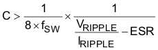
Equation 6. 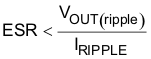
For this design, the minimum required capacitance is 8.45 µF and maximum ESR is 33 mΩ. Therefore, two TDK C3216JB0J226M 22-µF output capacitors are used. The maximum ESR is 12 mΩ for each capacitor.