JAJSC06C SEPTEMBER 2013 – June 2018 TPS53513
PRODUCTION DATA.
- 1 特長
- 2 アプリケーション
- 3 概要
- 4 改訂履歴
- 5 Pin Configuration and Functions
- 6 Specifications
-
7 Detailed Description
- 7.1 Overview
- 7.2 Functional Block Diagram
- 7.3
Feature Description
- 7.3.1 5-V LDO and VREG Start-Up
- 7.3.2 Enable, Soft Start, and Mode Selection
- 7.3.3 Frequency Selection
- 7.3.4 D-CAP3 Control and Mode Selection
- 7.3.5 Power-Good
- 7.3.6 Current Sense and Overcurrent Protection
- 7.3.7 Overvoltage and Undervoltage Protection
- 7.3.8 Out-Of-Bounds Operation
- 7.3.9 UVLO Protection
- 7.3.10 Thermal Shutdown
- 7.4 Device Functional Modes
- 8 Application and Implementation
- 9 Power Supply Recommendations
- 10Layout
- 11デバイスおよびドキュメントのサポート
- 12メカニカル、パッケージ、および注文情報
パッケージ・オプション
メカニカル・データ(パッケージ|ピン)
- RVE|28
サーマルパッド・メカニカル・データ
- RVE|28
発注情報
7.3.4.2 Sample and Hold Circuitry
 Figure 36. Sample and Hold Logic Circuitry (Patent Pending)
 The sample and hold circuitry is the difference between D-CAP3 and D-CAP2. The sample and hold circuitry, which is an advance control scheme to boost output voltage accuracy higher on the device, is one of features of the device. The sample and hold circuitry generates a new DC voltage of CSN instead of the voltage which is produced by RC2 and CC2 which allows for tight output-voltage accuracy and makes the device more competitive.
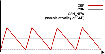 Figure 37. Continuous Conduction Mode (CCM) With Sample and Hold Circuitry
 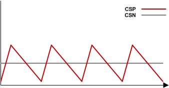 Figure 39. Continuous Conduction Mode (CCM) Without Sample and Hold Circuitry
 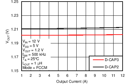 Figure 41. Output Voltage vs Output Current
 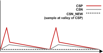 Figure 38. Discontinuous Conduction Mode (DCM) With Sample and Hold Circuitry
 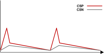 Figure 40. Discontinuous Conduction Mode (DCM) Without Sample and Hold Circuitry
 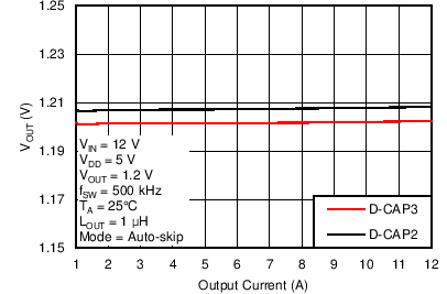 Figure 42. Output Voltage vs Output Current