JAJSK12C September 2020 – December 2021 TPS542A50
PRODUCTION DATA
- 1 特長
- 2 アプリケーション
- 3 概要
- 4 Revision History
- 5 Pin Configuration and Functions
- 6 Specifications
-
7 Detailed Description
- 7.1 Overview
- 7.2 Functional Block Diagram
- 7.3
Feature Description
- 7.3.1 Enable and Adjustable Undervoltage Lockout
- 7.3.2 Input and VREG Undervoltage Lockout Protection
- 7.3.3 Voltage Reference and Setting the Output Voltage
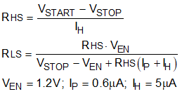
- 7.3.4 Remote Sense Function
- 7.3.5 Switching Frequency
- 7.3.6 Voltage Control Mode Internal Compensation
- 7.3.7 Soft Start and Prebiased Output Start-up
- 7.3.8 Power Good
- 7.3.9 Overvoltage and Undervoltage Protection
- 7.3.10 Overcurrent Protection
- 7.3.11 High-Side FET Throttling
- 7.3.12 Overtemperature Protection
- 7.4 Device Functional Modes
- 7.5 Programming
- 7.6 Pin-Strap Programming
- 7.7
Register Maps
- 7.7.1 ID Register (Offset = 0x0) [reset = 0x21]
- 7.7.2 STATUS Register (Offset = 0x1) [reset = 0x0]
- 7.7.3 VOUT_ADJ1 Register (Offset = 0x2) [reset = 0x0]
- 7.7.4 VOUT_ADJ2 Register (Offset = 0x3) [reset = 0x0]
- 7.7.5 CONFIG1 Register (Offset = 0x4) [reset = 0x0B]
- 7.7.6 CONFIG2 Register (Offset = 0x5) [reset = 0x2D]
-
8 Application and Implementation
- 8.1 Application Information
- 8.2
Typical Application
- 8.2.1
Full Analog Configuration
- 8.2.1.1 Design Requirements
- 8.2.1.2
Detailed Design Procedure
- 8.2.1.2.1 Custom Design With WEBENCH® Tools
- 8.2.1.2.2 Output Voltage Calculation
- 8.2.1.2.3 Switching Frequency Selection
- 8.2.1.2.4 Inductor Selection
- 8.2.1.2.5 Input Capacitor Selection
- 8.2.1.2.6 Bootstrap Capacitor Selection
- 8.2.1.2.7 R-C Snubber and VIN Pin High-Frequency Bypass
- 8.2.1.2.8 Output Capacitor Selection
- 8.2.1.2.9 Response to a Load Transient
- 8.2.1.2.10 Pin-Strap Setting
- 8.2.1.3 Application Curves
- 8.2.1.4 Typical Application Circuits
- 8.2.1
Full Analog Configuration
- 9 Power Supply Recommendations
- 10Layout
- 11Device and Documentation Support
- 12Mechanical, Packaging, and Orderable Information
7.3.1 Enable and Adjustable Undervoltage Lockout
The EN pin provides electrical on/off control of the device. Once the EN pin voltage exceeds the threshold voltage (typically 1.2 V), the device starts operation. If the EN pin voltage is pulled below the threshold voltage, the regulator stops switching and enters low power shutdown.
The EN pin has an internal pullup current source, allowing the user to float the EN pin for enabling the device. The EN pin can also be externally driven high or low. When the pulse-width is less than 22us, the EN pin will detect the pulse as a low and cause the device to enter hiccup-mode. If the pulse-width is greater than 22us, then the EN pin will detect the pulse as low but will not enter hiccup-mode.
For adjustable input undervoltage lockout (UVLO), connect the EN pin to the middle point of an external resistor divider. Once the EN pin voltage exceeds the threshold, an additional 5 µA of hystersis current is added to facilitate UVLO hysteresis. Equation 1 shows the calculation of resistor divider network.
 Figure 7-1 EN UVLO