SLVSD01B September 2015 – May 2019 TPS57140-EP
PRODUCTION DATA.
- 1 Features
- 2 Applications
- 3 Description
- 4 Revision History
- 5 Pin Configuration and Functions
- 6 Specifications
-
7 Detailed Description
- 7.1 Overview
- 7.2 Functional Block Diagram
- 7.3
Feature Description
- 7.3.1 Fixed Frequency PWM Control
- 7.3.2 Slope-Compensation Output Current
- 7.3.3 Bootstrap Voltage (Boot)
- 7.3.4 Low-Dropout Operation
- 7.3.5 Error Amplifier
- 7.3.6 Voltage Reference
- 7.3.7 Adjusting the Output Voltage
- 7.3.8 Enable and Adjusting UVLO
- 7.3.9 Slow-Start or Tracking Pin (SS/TR)
- 7.3.10 Overload Recovery Circuit
- 7.3.11 Constant Switching Frequency and Timing Resistor (RT/CLK Pin)
- 7.3.12 Overcurrent Protection and Frequency Shift
- 7.3.13 Selecting the Switching Frequency
- 7.3.14 How to Interface to RT/CLK Pin
- 7.3.15 Power Good (PWRGD Pin)
- 7.3.16 Overvoltage Transient Protection (OVTP)
- 7.3.17 Thermal Shutdown
- 7.3.18 Small-Signal Model for Loop Response
- 7.3.19 Simple Small-Signal Model for Peak-Current-Mode Control
- 7.3.20 Small-Signal Model for Frequency Compensation
- 7.4 Device Functional Modes
-
8 Application and Implementation
- 8.1 Application Information
- 8.2
Typical Application
- 8.2.1 Design Requirements
- 8.2.2
Detailed Design Procedure
- 8.2.2.1 Selecting the Switching Frequency
- 8.2.2.2 Output Inductor Selection (LO)
- 8.2.2.3 Output Capacitor
- 8.2.2.4 Catch Diode
- 8.2.2.5 Input Capacitor
- 8.2.2.6 Slow-Start Capacitor
- 8.2.2.7 Bootstrap Capacitor Selection
- 8.2.2.8 UVLO Set Point
- 8.2.2.9 Output Voltage and Feedback Resistors Selection
- 8.2.2.10 Compensation
- 8.2.3 Application Curves
- 9 Power Supply Recommendations
- 10Layout
- 11Device and Documentation Support
- 12Mechanical, Packaging, and Orderable Information
パッケージ・オプション
メカニカル・データ(パッケージ|ピン)
- DRC|10
サーマルパッド・メカニカル・データ
- DRC|10
発注情報
7.3.11 Constant Switching Frequency and Timing Resistor (RT/CLK Pin)
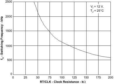
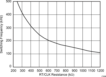
The switching frequency of the TPS57140-EP is adjustable over a wide range from approximately 100-kHz to 2500-kHz by placing a resistor on the RT/CLK pin. The RT/CLK pin voltage is typically 0.5 V and must have a resistor to ground to set the switching frequency. To determine the timing resistance for a given switching frequency, use Equation 7 or the curves in Figure 32 or Figure 33. To reduce the solution size, the designer would typically set the switching frequency as high as possible, but consider tradeoffs of the supply efficiency, maximum input voltage, and minimum controllable on-time.
The minimum controllable on time is typically 130 ns, which limits the maximum operating input voltage.
The frequency-shift circuit also limits the maximum switching frequency. The following contains more discussion on the details of the maximum switching frequency.


