SLVSD01B September 2015 – May 2019 TPS57140-EP
PRODUCTION DATA.
- 1 Features
- 2 Applications
- 3 Description
- 4 Revision History
- 5 Pin Configuration and Functions
- 6 Specifications
-
7 Detailed Description
- 7.1 Overview
- 7.2 Functional Block Diagram
- 7.3
Feature Description
- 7.3.1 Fixed Frequency PWM Control
- 7.3.2 Slope-Compensation Output Current
- 7.3.3 Bootstrap Voltage (Boot)
- 7.3.4 Low-Dropout Operation
- 7.3.5 Error Amplifier
- 7.3.6 Voltage Reference
- 7.3.7 Adjusting the Output Voltage
- 7.3.8 Enable and Adjusting UVLO
- 7.3.9 Slow-Start or Tracking Pin (SS/TR)
- 7.3.10 Overload Recovery Circuit
- 7.3.11 Constant Switching Frequency and Timing Resistor (RT/CLK Pin)
- 7.3.12 Overcurrent Protection and Frequency Shift
- 7.3.13 Selecting the Switching Frequency
- 7.3.14 How to Interface to RT/CLK Pin
- 7.3.15 Power Good (PWRGD Pin)
- 7.3.16 Overvoltage Transient Protection (OVTP)
- 7.3.17 Thermal Shutdown
- 7.3.18 Small-Signal Model for Loop Response
- 7.3.19 Simple Small-Signal Model for Peak-Current-Mode Control
- 7.3.20 Small-Signal Model for Frequency Compensation
- 7.4 Device Functional Modes
-
8 Application and Implementation
- 8.1 Application Information
- 8.2
Typical Application
- 8.2.1 Design Requirements
- 8.2.2
Detailed Design Procedure
- 8.2.2.1 Selecting the Switching Frequency
- 8.2.2.2 Output Inductor Selection (LO)
- 8.2.2.3 Output Capacitor
- 8.2.2.4 Catch Diode
- 8.2.2.5 Input Capacitor
- 8.2.2.6 Slow-Start Capacitor
- 8.2.2.7 Bootstrap Capacitor Selection
- 8.2.2.8 UVLO Set Point
- 8.2.2.9 Output Voltage and Feedback Resistors Selection
- 8.2.2.10 Compensation
- 8.2.3 Application Curves
- 9 Power Supply Recommendations
- 10Layout
- 11Device and Documentation Support
- 12Mechanical, Packaging, and Orderable Information
パッケージ・オプション
メカニカル・データ(パッケージ|ピン)
- DRC|10
サーマルパッド・メカニカル・データ
- DRC|10
発注情報
7.3.4 Low-Dropout Operation
The voltage drops across the power MOSFET, inductor, low-side diode, and PCB resistance mainly determine the duty cycle during dropout of the regulator. During operating conditions in which the input voltage drops, the high-side MOSFET can remain on for 100% of the duty cycle to maintain output regulation until the BOOT-to-PH voltage falls below 2.1 V.
After the high side is off, the low-side diode conducts and the BOOT capacitor recharges. During this boot-capacitor recharge time, the inductor current ramps down until the high-side MOSFET turns on. The recharge time is longer than the typical high-side off-time of previous switching cycles, and thus the inductor-current ripple is larger, resulting in more ripple voltage on the output. The recharge time is a function of the input voltage, boot-capacitor value, and the impedance of the internal boot-recharge diode.
Pay attention in maximum-duty-cycle applications which experience extended time periods without a load current. When the voltage across the BOOT capacitors falls below the 2.1-V threshold in applications that have a difference in the input voltage and output voltage that is <3 V, the high-side MOSFET turns off, but there is not enough current in the inductor to pull the PH pin down to recharge the boot capacitor. The regulator does not switch because the boot capacitor is less than 2.1 V, and the output capacitor decays until the difference between the input voltage and output voltage is 2.1 V. At this time, the boot UVLO is exceeded and the device switches until reaching the desired output voltage.
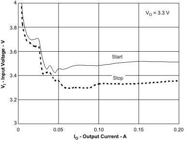
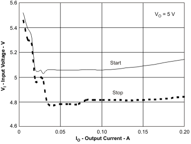
Figure 26 and Figure 27 show the start and stop voltages for 3.3-V and 5-V applications. The graphs plot voltages versus the load current. The definition of start voltage is the input voltage needed to regulate within 1%. The definition of stop voltage is the input voltage at which the output drops by 5% or stops switching.

