JAJS467F December 2008 – April 2019 TPS61175
PRODUCTION DATA.
- 1 特長
- 2 アプリケーション
- 3 概要
- 4 改訂履歴
- 5 Pin Configuration and Functions
- 6 Specifications
- 7 Detailed Description
-
8 Application and Implementation
- 8.1 Application Information
- 8.2
Typical Application
- 8.2.1 Design Requirements
- 8.2.2
Detailed Design Procedure
- 8.2.2.1 Custom Design with WEBENCH Tools
- 8.2.2.2 Determining the Duty Cycle
- 8.2.2.3 Selecting the Inductor
- 8.2.2.4 Computing the Maximum Output Current
- 8.2.2.5 Setting Output Voltage
- 8.2.2.6 Setting the Switching Frequency
- 8.2.2.7 Setting the Soft-Start Time
- 8.2.2.8 Selecting the Schottky Diode
- 8.2.2.9 Selecting the Input and Output Capacitors
- 8.2.2.10 Compensating the Small Signal Control Loop
- 8.2.3 Application Curves
- 9 Power Supply Recommendations
- 10Layout
- 11デバイスおよびドキュメントのサポート
- 12メカニカル、パッケージ、および注文情報
パッケージ・オプション
メカニカル・データ(パッケージ|ピン)
- PWP|14
サーマルパッド・メカニカル・データ
- PWP|14
発注情報
7.3.1 Switching Frequency
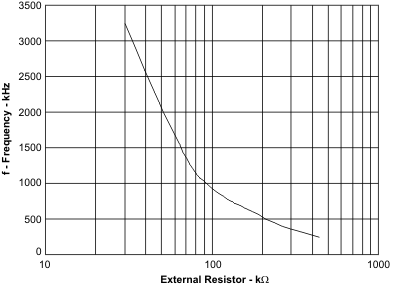
The switch frequency is set by a resistor (R4) connected to the FREQ pin of the TPS61175. Do not leave this pin open. A resistor must always be connected for proper operation. See Table 2 and Figure 7 for resistor values and corresponding frequencies.
Table 2. Switching Frequency vs External Resistor
| R4 (kΩ) | fSW (kHz) |
|---|---|
| 443 | 240 |
| 256 | 400 |
| 176 | 600 |
| 80 | 1200 |
| 51 | 2000 |
 Figure 7. Switching Frequency vs External Resistor
 Alternatively, the TPS61175 switching frequency will synchronize to an external clock signal that is applied to the SYNC pin. The logic level of the external clock is shown in the specification table. The duty cycle of the clock is recommended in the range of 10% to 90%. The resistor also must be connected to the FREQ pin when IC is switching by the external clock. The external clock frequency must be within ±20% of the corresponding frequency set by the resistor. For example, if the corresponding frequency as set by a resistor on the FREQ pin is 1.2-MHz, the external clock signal should be in the range of 0.96 MHz to 1.44 MHz.
If the external clock signal is higher than the frequency per the resistor on the FREQ pin, the maximum duty cycle specification (DMAX) should be lowered by 2%. For instance, if the resistor set value is 2.5 MHz, and the external clock is 3 MHz, DMAX is 87% instead of 89%.