SLVSBX9A September 2014 – September 2014 TPS61291
PRODUCTION DATA.
- 1 Features
- 2 Applications
- 3 Description
- 4 Revision History
- 5 Pin Configuration and Functions
- 6 Specifications
- 7 Detailed Description
- 8 Applications and Implementation
- 9 Power Supply Recommendations
- 10Layout
- 11Device and Documentation Support
- 12Mechanical, Packaging, and Orderable Information
パッケージ・オプション
メカニカル・データ(パッケージ|ピン)
- DRV|6
サーマルパッド・メカニカル・データ
- DRV|6
発注情報
7 Detailed Description
7.1 Overview
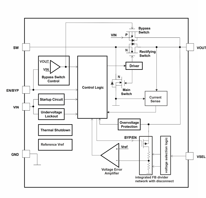
The TPS61291 provides two operating modes: high efficiency boost mode to generate an output voltage higher than the input voltage and bypass mode, which connects the output of the device directly to the input.
7.2 Functional Block Diagram
7.3 Feature Description
7.3.1 Bypass / Boost Mode Operation EN/BYP
The EN/BYP pin selects the operating mode of the device. With the EN/BYP pin pulled low, the device operates in bypass mode. With a high level on the EN/BYP pin, the device operates as a boost converter. The EN/BYP pin is usually controlled by an I/O pin of a MCU, powered from the output of the TPS61291 and should not be left floating. See Figure 8. See also sections Boost Mode Operation and Bypass Mode Operation for more detailed descriptions.
7.3.2 Output Voltage Selection VSEL
In boost mode operation, the device supports three internally set output voltages: 2.5V, 3V and 3.3V. Leaving the VSEL pin open sets the output voltage to 2.5V, VSEL = VOUT to 3.0V and VSEL= GND to 3.3V. The VSEL pin condition is detected during the startup of the boost converter and internally latched. For proper operation, it must be connected to either GND, VOUT or left floating. Depending on the VSEL condition, an integrated feedback divider network is selected. Changing the VSEL pin condition during operation does not change the output voltage.
7.3.3 Feedback Divider Disconnect
In boost mode operation, the integrated feedback divider network, which is required for regulation, is connected to the VOUT pin. To achieve the low quiescent current in bypass mode, the integrated feedback divider network is disconnected from the output pin VOUT.
7.3.4 Undervoltage Lockout
An undervoltage lockout function stops the operation of the boost converter if the input voltage drops below the undervoltage lockout threshold. This function is implemented in order to prevent malfunction of the boost converter. The undervoltage lockout function has no control of the bypass switch.
7.3.5 Overtemperature Protection
The device has a built-in temperature sensor which monitors the internal junction temperature in boost mode operation. If the junction temperature exceeds the threshold (140 °C typical), the device stops operating. As soon as the junction temperature has decreased below the programmed threshold, it starts operating again. There is a built-in hysteresis to avoid unstable operation at IC temperatures at the overtemperature threshold. The overtemperature protection is not active in bypass mode operation.
7.3.6 Overvoltage Protection
In boost mode operation (EB/BYP = high), the device features a redundant over voltage protection circuit (OVP), which is independent from the reference, the regulation loop and feedback divider network. The redundant over voltage protection circuit limits the output voltage to typically 5.4V. The over voltage protection can only limit the output voltage in boost mode operation, when the input voltage VIN is smaller than the output voltage VOUT.
7.4 Device Functional Modes
7.4.1 Boost Mode Operation
The device is enabled and operates in boost mode operation when the EN/BYP pin is set high. The bypass switch is turned off once the boost converter has started switching.
In boost mode operation, the device is controlled by a hysteretic current mode controller. This controller regulates the output voltage by keeping the inductor ripple current constant in the range of 300 mA and adjusting the offset of this inductor current depending on the output load. If the required average input current is lower than the average inductor current defined by this constant ripple, the inductor current goes discontinuous to keep the efficiency high at low load conditions. To achieve high efficiency, the power stage is realized as a synchronous boost topology.
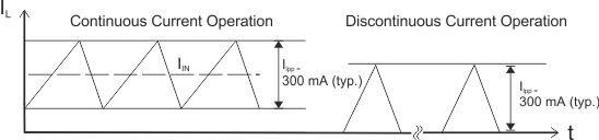 Figure 7. Hysteretic Current Operation
The output voltage VOUT is monitored via the integrated feedback network which is connected to the voltage error amplifier. To regulate the output voltage, the voltage error amplifier compares this feedback voltage to the internal voltage reference and adjusts the required offset of the inductor current accordingly.
The hysteretic current mode architecture allows fast response to load variations.
7.4.2 Bypass Mode Operation
The TPS61291 includes a P-channel MOSFET (Bypass Switch) between the VIN and VOUT pins. When the IC is disabled (EN/BYP = low), bypass mode is activated to provide a direct, low impedance connection from the input voltage (at the VIN pin) to the load (VOUT). The bypass switch is not impacted by undervoltage lockout, or thermal shutdown. The bypass switch is not current-limit controlled. In bypass operation, the OVP circuit is disabled.
7.4.3 Controlled Transition into Bypass Mode
When changing from boost mode into bypass mode, the output capacitor is usually charged up to a higher voltage than the battery voltage VBAT. In order to prevent current flowing from the output capacitor COUT via the bypass switch into the battery (reverse battery current), the internal bypass control circuit delays the bypass switch activation until the output voltage VOUT has decreased to the input voltage level.
7.4.4 Operation at Output Overload
If the peak inductor current reaches the internal switch current limit threshold in boost mode operation, the main switch is turned off to stop a further increase of the input current. In this case the output voltage will decrease since the device cannot provide sufficient power to maintain the set output voltage. If the output voltage drops below the input voltage, the backgate diode of the rectifying switch gets forward biased and current starts to flow through it. Because this diode cannot be turned off, the load current is only limited by the remaining DC resistance. As soon as the overload condition is removed, the converter automatically resumes normal operation and enters the appropriate soft start mode depending on the operating conditions.
7.4.5 Startup
After the EN/BYP pin is tied high, the device starts to operate. If the input voltage is not high enough to supply the control circuit properly, a startup oscillator starts to operate the switches. During this phase, the switching frequency is controlled by the oscillator and the switch current is limited. As soon as the device has built up the output voltage to about 1.8 V, high enough for supplying the control circuit, the device switches to its normal hysteretic current mode operation.