JAJSE91A September 2017 – December 2017 TPS62097-Q1
PRODUCTION DATA.
- 1 特長
- 2 アプリケーション
- 3 概要
- 4 改訂履歴
- 5 Terminal Configuration and Functions
- 6 Specifications
- 7 Detailed Description
- 8 Application Information
- 9 Power Supply Recommendations
- 10PCB Layout
- 11デバイスおよびドキュメントのサポート
- 12メカニカル、パッケージ、および注文情報
パッケージ・オプション
デバイスごとのパッケージ図は、PDF版データシートをご参照ください。
メカニカル・データ(パッケージ|ピン)
- RGT|16
サーマルパッド・メカニカル・データ
発注情報
10 PCB Layout
10.1 Layout Guidelines
- TI recommends to place all components as close as possible to the IC. Specially, the input capacitor placement must be closest to the PVIN and PGND pins of the device.
- The low side of the input and output capacitors must be connected directly to the PGND pin to avoid a ground potential shift.
- Use wide and short traces for the main current paths to reduce the parasitic inductance and resistance.
- The sense trace connected to VOS pin is a signal trace. Special care should be taken to avoid noise being induced. Keep the trace away from SW nodes.
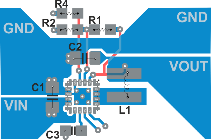
- Refer to Figure 25 for an example of component placement, routing and thermal design.
10.2 Layout Example
 Figure 25. TPS62097-Q1 PCB Layout
10.3 Thermal Information
Implementation of integrated circuits in low-profile and fine pitch surface mount packages typically requires special attention to power dissipation. Many system dependent issues such as thermal coupling, airflow, added heat sinks and convection surfaces, and the presence of other heat-generating components affect the power-dissipation limits of a given component. For more details on how to use the thermal parameters, see the application notes: Thermal Characteristics Application Notes SZZA017 and SPRA953.