JAJSE91A September 2017 – December 2017 TPS62097-Q1
PRODUCTION DATA.
- 1 特長
- 2 アプリケーション
- 3 概要
- 4 改訂履歴
- 5 Terminal Configuration and Functions
- 6 Specifications
- 7 Detailed Description
- 8 Application Information
- 9 Power Supply Recommendations
- 10PCB Layout
- 11デバイスおよびドキュメントのサポート
- 12メカニカル、パッケージ、および注文情報
パッケージ・オプション
デバイスごとのパッケージ図は、PDF版データシートをご参照ください。
メカニカル・データ(パッケージ|ピン)
- RGT|16
サーマルパッド・メカニカル・データ
発注情報
8 Application Information
NOTE
Information in the following applications sections is not part of the TI component specification, and TI does not warrant its accuracy or completeness. TI’s customers are responsible for determining suitability of components for their purposes. Customers should validate and test their design implementation to confirm system functionality.
8.1 Application Information
The following section discusses the design of the external components to complete the power supply design of the TPS62097-Q1.
8.2 1.8-V Output Application
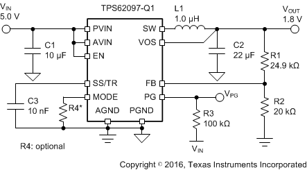 Figure 6. 1.8-V Output Application Schematic
8.2.1 Design Requirements
For this design example, use the following as the input parameters.
Table 3. Design Parameters
| DESIGN PARAMETER | EXAMPLE VALUE |
|---|---|
| Input voltage range | 2.5 V to 6 V |
| Output voltage | 1.8 V |
| Output current | 2.0 A |
Table 4 lists the components used for the example.
Table 4. List of Components
| REFERENCE | DESCRIPTION | MANUFACTURER(1) |
|---|---|---|
| C1 | 10 μF, Ceramic Capacitor, 6.3V, X7R, size 0805, C2012X7R0J106M125AB | TDK |
| C2 | 22 μF, Ceramic Capacitor, 6.3V, X7S, size 0805, C2012X7S1A226M125AC | TDK |
| C3 | 10 nF, Ceramic Capacitor, 6.3V, X7R, size 0603, GRM188R70J103KA01 | Murata |
| L1 | 1 µH, Shielded, 5.4A, XFL4020-102MEB | Coilcraft |
| R1 | Depending on the output voltage, 1% accuracy | Std |
| R2 | 20 kΩ, 1% accuracy | Std |
| R3 | 100 kΩ, 1% accuracy | Std |
8.2.2 Detailed Design Procedure
8.2.2.1 Setting the Output Voltage
The output voltage is set by an external resistor divider according to the following equation:

R2 should not be higher than 20 kΩ to reduce noise coupling into the FB pin and improve the output voltage regulation. Choose additional resistor values for other outputs. A feed forward capacitor is not required.
The fixed output voltage version, TPS6209733-Q1, does not need an external resistor divider. TI recommends to connect the FB pin to AGND for improved thermal performance.
8.2.2.2 Output Filter Design
The inductor and the output capacitor together provide a low-pass filter. To simplify the selection process, Table 5 outlines possible inductor and capacitor value combinations for most applications.
Table 5. Output Capacitor / Inductor Combinations
| NOMINAL L [µH](2) | NOMINAL COUT [µF](3) | ||||
|---|---|---|---|---|---|
| 10 | 22 | 47 | 100 | 150 | |
| 0.47 | |||||
| 1 | +(1) | + | + | + | |
| 2.2 | |||||
8.2.2.3 Inductor Selection
The main parameters for the inductor selection are the inductor value and the saturation current. To calculate the maximum inductor current under static load conditions, Equation 5 is given.
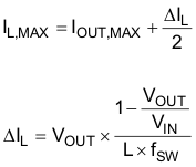
Where:
IOUT,MAX = Maximum output current
ΔIL = Inductor current ripple
fSW = Switching frequency
L = Inductor value
TI recommends to choose the saturation current for the inductor 20% to 30% higher than the IL,MAX, out of Equation 5. A higher inductor value is also useful to lower ripple current but increases the transient response time as well.
8.2.2.4 Capacitor Selection
The input capacitor is the low impedance energy source for the converters which helps to provide stable operation. A low ESR multilayer ceramic capacitor is required for best filtering and should be placed between PVIN and PGND as close as possible to those pins. For most applications a 10-μF capacitor is sufficient, though a larger value reduces input current ripple.
The architecture of the TPS62097-Q1 allows the use of tiny ceramic output capacitors with low equivalent series resistance (ESR). These capacitors provide low output voltage ripple and are recommended. To keep its low resistance up to high frequencies and to get narrow capacitance variation with temperature, TI recommends to use X7R or X5R dielectrics. The recommended typical output capacitor value is 22 μF and can vary over a wide range as outlined in Table 5.
Ceramic capacitors have a DC-Bias effect, which has a strong influence on the final effective capacitance. Choose the right capacitor carefully in combination with considering its package size and voltage rating. Ensure that the input effective capacitance is at least 5 μF and the output effective capacitance is at least 10 μF.
8.2.3 Application Performance Curves
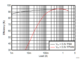
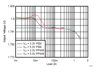
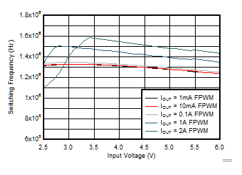
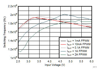
TA = 25°C, BOM = Table 4 unless otherwise noted.
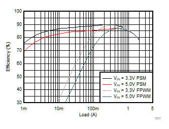
| VOUT = 1.0 V | FSW = 2.0 MHz |
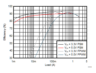
| VOUT = 1.8 V | FSW = 2.0 MHz |
| VOUT = 3.3 V | FSW = 2.0 MHz |
| VOUT = 1.0 V | RMode = 8.2 kΩ |
| VOUT = 1.0 V | MODE = Open |
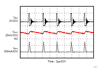
| VOUT = 1.2 V | IOUT = 30 mA |
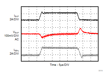
| VOUT = 1.2 V | IOUT = 0 A to 2 A, 1A / µs | |
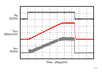
| VOUT = 1.2 V | ROUT = 0.6 Ω (2 A) |

| VOUT = 1.2 V | FSW = 2.0 MHz |
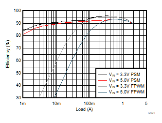
| VOUT = 2.5 V | FSW = 2.0 MHz |
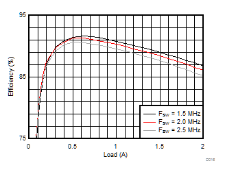
| VOUT = 1.8 V | VIN = 5.0 V |
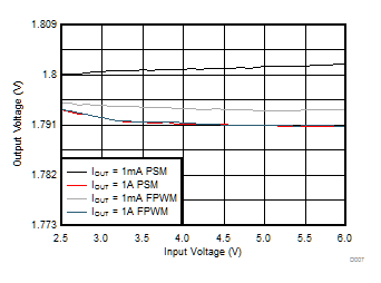
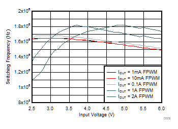
| VOUT = 1.0 V | MODE = AGND, Forced PWM | |
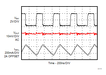
| VOUT = 1.2 V | IOUT = 2 A |
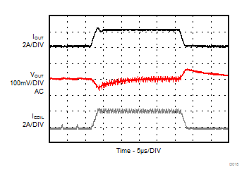
| VOUT = 1.2 V | IOUT = 0 A to 2 A, 1A / µs | |
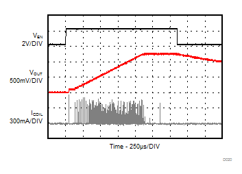
| VOUT = 1.2 V | ROUT = No Load |
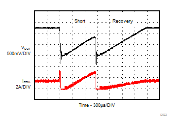
| VOUT = 1.2 V | ROUT = 0.8 Ω (1.5 A) with 1-ms short | |