JAJSQ70D january 2014 – may 2023 TPS65262
PRODUCTION DATA
- 1
- 1 特長
- 2 アプリケーション
- 3 概要
- 4 Revision History
- 5 Pin Configuration and Functions
- 6 Specifications
-
7 Detailed Description
- 7.1 Overview
- 7.2 Functional Block Diagram
- 7.3
Feature Description
- 7.3.1 Adjusting the Output Voltage
- 7.3.2 Enable and Adjusting Undervoltage Lockout
- 7.3.3 Soft-Start Time
- 7.3.4 Power-Up Sequencing
- 7.3.5 V7V Low Dropout Regulator and Bootstrap
- 7.3.6 Out-of-Phase Operation
- 7.3.7 Output Overvoltage Protection (OVP)
- 7.3.8 PSM
- 7.3.9 Slope Compensation
- 7.3.10 Overcurrent Protection
- 7.3.11 Power Good
- 7.3.12 Thermal Shutdown
- 7.4 Device Functional Modes
- 8 Application and Implementation
- 9 Device and Documentation Support
- 10Mechanical, Packaging, and Orderable Information
パッケージ・オプション
メカニカル・データ(パッケージ|ピン)
- RHB|32
サーマルパッド・メカニカル・データ
- RHB|32
発注情報
8.2.2.4 Loop Compensation
The TPS65262 incorporates a peak current mode control scheme. The error amplifier is a transconductance amplifier with a gain of 300 µS. A typical type II compensation circuit adequately delivers a phase margin between 60° to 90°. Cb adds a high-frequency pole to attenuate high frequency noise when needed. To calculate the external compensation components, follow the following steps.
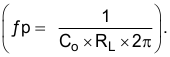
- Switching frequency ƒsw 600 kHz is appropriate for application depending on L and C sizes, output ripple, EMI, and so forth, also gives best trade-off between performance and cost.
- Set up crossover frequency, ƒc, which is typically between 1/5 and 1/20 of ƒsw.
- RC can be determined by
Equation 16.
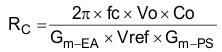
Where Gm_EA is the error amplifier gain (300 µS), Gm_PS is the power stage voltage to current conversion gain (7.4 A/V).
- Calculate CC by placing a compensation zero at or before the dominant pole
 Equation 17.
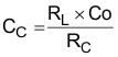
- Optional Cb can be used to cancel the zero from the ESR associated with CO.
Equation 18.
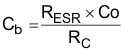
 Figure 8-2 DC/DC Loop Compensation