SLVSC27D July   2013  – October 2016 TPS65631W

PRODUCTION DATA.  

  1. Features
  2. Applications
  3. Description
  4. Simplified Schematic
  5. Revision History
  6. Pin Configuration and Functions
  7. Specifications
    1. 7.1 Absolute Maximum Ratings
    2. 7.2 ESD Ratings
    3. 7.3 Recommended Operating Conditions
    4. 7.4 Thermal Information
    5. 7.5 Electrical Characteristics
    6. 7.6 Timing Requirements
    7. 7.7 Typical Characteristics
  8. Detailed Description
    1. 8.1 Overview
    2. 8.2 Functional Block Diagram
    3. 8.3 Feature Description
      1. 8.3.1 Boost Converter
      2. 8.3.2 Inverting Buck-Boost Converter
      3. 8.3.3 Soft-Start and Start-Up Sequence
      4. 8.3.4 Enable (CTRL)
      5. 8.3.5 Undervoltage Lockout
      6. 8.3.6 Short Circuit Protection
        1. 8.3.6.1 Short-Circuits During Normal Operation
        2. 8.3.6.2 Short-Circuits During Start-Up
      7. 8.3.7 Thermal Shutdown
    4. 8.4 Device Functional Modes
      1. 8.4.1 Operation with VI < 2.9 V
      2. 8.4.2 Operation with VI ≈ VPOS (Diode Mode)
      3. 8.4.3 Operation with CTRL
    5. 8.5 Programming
      1. 8.5.1 Programming VNEG
  9. Applications and Implementation
    1. 9.1 Application Information
    2. 9.2 Typical Application
      1. 9.2.1 Design Requirements
      2. 9.2.2 Detailed Design Procedure
        1. 9.2.2.1 Inductor Selection
        2. 9.2.2.2 Capacitor Selection
        3. 9.2.2.3 Stability
      3. 9.2.3 Application Curves
  10. 10Power Supply Recommendations
  11. 11Layout
    1. 11.1 Layout Guidelines
    2. 11.2 Layout Example
  12. 12Device and Documentation Support
    1. 12.1 Device Support
      1. 12.1.1 Third-Party Products Disclaimer
    2. 12.2 Receiving Notification of Documentation Updates
    3. 12.3 Community Resources
    4. 12.4 Trademarks
    5. 12.5 Electrostatic Discharge Caution
    6. 12.6 Glossary
  13. 13Mechanical, Packaging, and Orderable Information

パッケージ・オプション

メカニカル・データ(パッケージ|ピン)
サーマルパッド・メカニカル・データ
発注情報

11 Layout

11.1 Layout Guidelines

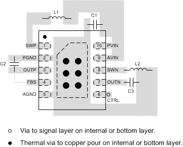
No PCB layout is perfect and compromises are always necessary. However, following the basic principles listed below (in order of importance) should go a long way to achieving good performance:

  • Route switching currents on the top layer using short, wide traces. Do not route these signals through vias, which have relatively high parasitic inductance and resistance.
  • Use a copper pour on layer 2 as a ground plane and thermal spreader, and connect the thermal pad to it using a number of thermal vias.
  • Place C1 as close as possible to pin 10.
  • Place C2 as close as possible to pins 2 and 3.
  • Place C3 as close as possible to pin 7.
  • Place L1 as close as possible to pin 1.
  • Place L2 as close as possible to pin 10.
  • Use the thermal pad to join AGND and PGND.
  • Connect the FBS pin directly to the positive pin of C2, that is, keep this connection separate from the connection between OUTP and C2.

Figure 23 illustrates how a PCB layout following the above principles may be realized in practice.
11.2 Layout Example

Figure 23 shows the above principles implemented for the circuit of Figure 8.

TPS65631W Layout_01_TPS65631W.gif Figure 23. PCB Layout Example