JAJSLW7B December 2020 – September 2023 TPS6593-Q1
PRODUCTION DATA
- 1
- 1 特長
- 2 アプリケーション
- 3 概要
- 4 Revision History
- 5 概要 (続き)
- 6 Pin Configuration and Functions
-
7 Specifications
- 7.1 Absolute Maximum Ratings
- 7.2 ESD Ratings
- 7.3 Recommended Operating Conditions
- 7.4 Thermal Information
- 7.5 General Purpose Low Drop-Out Regulators (LDO1, LDO2, LDO3)
- 7.6 Low Noise Low Drop-Out Regulator (LDO4)
- 7.7 Internal Low Drop-Out Regulators (LDOVRTC, LDOVINT)
- 7.8 BUCK1, BUCK2, BUCK3, BUCK4 and BUCK5 Regulators
- 7.9 Reference Generator (BandGap)
- 7.10 Monitoring Functions
- 7.11 Clocks, Oscillators, and PLL
- 7.12 Thermal Monitoring and Shutdown
- 7.13 System Control Thresholds
- 7.14 Current Consumption
- 7.15 Backup Battery Charger
- 7.16 Digital Input Signal Parameters
- 7.17 Digital Output Signal Parameters
- 7.18 I/O Pullup and Pulldown Resistance
- 7.19 I2C Interface
- 7.20 Serial Peripheral Interface (SPI)
- 7.21 Typical Characteristics
-
8 Detailed Description
- 8.1 Overview
- 8.2 Functional Block Diagram
- 8.3
Feature Description
- 8.3.1 System Supply Voltage Monitor
- 8.3.2
Power Resources (Bucks and LDOs)
- 8.3.2.1
Buck Regulators
- 8.3.2.1.1 BUCK Regulator Overview
- 8.3.2.1.2 Multi-Phase Operation and Phase-Adding or Shedding
- 8.3.2.1.3 Transition Between PWM and PFM Modes
- 8.3.2.1.4 Multi-Phase BUCK Regulator Configurations
- 8.3.2.1.5 Spread-Spectrum Mode
- 8.3.2.1.6 Adaptive Voltage Scaling (AVS) and Dynamic Voltage Scaling (DVS) Support
- 8.3.2.1.7 BUCK Output Voltage Setting
- 8.3.2.1.8 BUCK Regulator Current Limit
- 8.3.2.1.9 SW_Bx Short-to-Ground Detection
- 8.3.2.1.10 Sync Clock Functionality
- 49
- 8.3.2.2 Low Dropout Regulators (LDOs)
- 8.3.2.1
Buck Regulators
- 8.3.3 Output Voltage Monitor and PGOOD Generation
- 8.3.4 Thermal Monitoring
- 8.3.5 Backup Supply Power-Path
- 8.3.6 General-Purpose I/Os (GPIO Pins)
- 8.3.7 nINT, EN_DRV, and nRSTOUT Pins
- 8.3.8 Interrupts
- 8.3.9 RTC
- 8.3.10
Watchdog (WDOG)
- 8.3.10.1 Watchdog Fail Counter and Status
- 8.3.10.2 Watchdog Start-Up and Configuration
- 8.3.10.3 MCU to Watchdog Synchronization
- 8.3.10.4 Watchdog Disable Function
- 8.3.10.5 Watchdog Sequence
- 8.3.10.6 Watchdog Trigger Mode
- 8.3.10.7 WatchDog Flow Chart and Timing Diagrams in Trigger Mode
- 79
- 8.3.10.8 Watchdog Question-Answer Mode
- 8.3.11 Error Signal Monitor (ESM)
- 8.4
Device Functional Modes
- 8.4.1
Device State Machine
- 8.4.1.1 Fixed Device Power FSM
- 8.4.1.2
Pre-Configurable Mission States
- 8.4.1.2.1
PFSM Commands
- 8.4.1.2.1.1 REG_WRITE_IMM Command
- 8.4.1.2.1.2 REG_WRITE_MASK_IMM Command
- 8.4.1.2.1.3 REG_WRITE_MASK_PAGE0_IMM Command
- 8.4.1.2.1.4 REG_WRITE_BIT_PAGE0_IMM Command
- 8.4.1.2.1.5 REG_WRITE_WIN_PAGE0_IMM Command
- 8.4.1.2.1.6 REG_WRITE_VOUT_IMM Command
- 8.4.1.2.1.7 REG_WRITE_VCTRL_IMM Command
- 8.4.1.2.1.8 REG_WRITE_MASK_SREG Command
- 8.4.1.2.1.9 SREG_READ_REG Command
- 8.4.1.2.1.10 SREG_WRITE_IMM Command
- 8.4.1.2.1.11 WAIT Command
- 8.4.1.2.1.12 DELAY_IMM Command
- 8.4.1.2.1.13 DELAY_SREG Command
- 8.4.1.2.1.14 TRIG_SET Command
- 8.4.1.2.1.15 TRIG_MASK Command
- 8.4.1.2.1.16 END Command
- 8.4.1.2.2 Configuration Memory Organization and Sequence Execution
- 8.4.1.2.3 Mission State Configuration
- 8.4.1.2.4 Pre-Configured Hardware Transitions
- 8.4.1.2.1
PFSM Commands
- 8.4.1.3 Error Handling Operations
- 8.4.1.4 Device Start-up Timing
- 8.4.1.5 Power Sequences
- 8.4.1.6 First Supply Detection
- 8.4.1.7 Register Power Domains and Reset Levels
- 8.4.2 Multi-PMIC Synchronization
- 8.4.1
Device State Machine
- 8.5 Control Interfaces
- 8.6 Configurable Registers
- 8.7 Register Maps
- 9 Application and Implementation
- 10Device and Documentation Support
- 11Mechanical, Packaging, and Orderable Information
パッケージ・オプション
メカニカル・データ(パッケージ|ピン)
- RWE|56
サーマルパッド・メカニカル・データ
- RWE|56
発注情報
8.3.1 System Supply Voltage Monitor
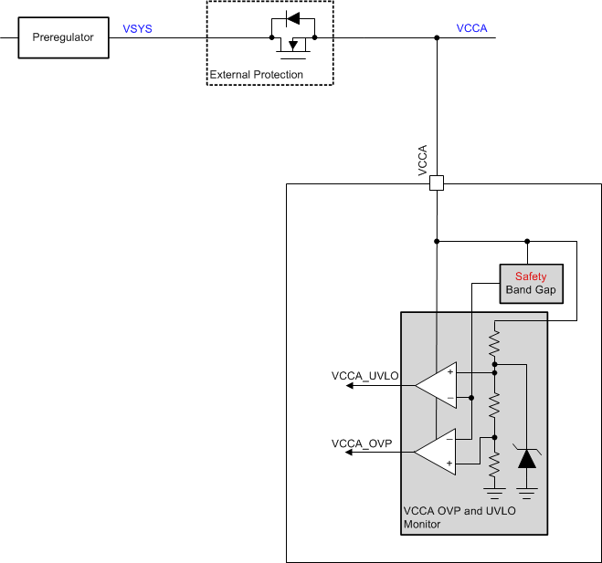
The comparator module in TPS6593-Q1, which monitors the voltage on the VCCA pins, controls the power state machine of the device. VCCA voltage detection outputs determine the power states of the device as follows:
-
VCCA_UVLO
The TPS6593-Q1
returns to the BACKUP state. LDOVRTC is
powered by the output of the Backup Supply Management (BSM) module
during the BACKUP state. The device returns to the NO SUPPLY
state and is completely shut down when the input supply of the LDOVRTC
falls below the operating range. The
device cannot return to the BACKUP state from the NO SUPPLY
state.
-
VCCA_UV
The TPS6593-Q1 transitions from the NO SUPPLY
state to the INIT state when the voltage on the VCCA pin rises above
VCCA_UV during initial power-up.
-
VCCA_OVP
If the voltage on VCCA pin rises above the VCCA_OVP threshold while TPS6593-Q1 is in operation, then the device clears the ENABLE_DRV bit and
starts the immediate shutdown sequence.
A separate voltage comparator monitors whether or not the VCCA voltage is within the expected PGOOD range when VCCA is expected to be 5-V or 3.3-V. This voltage comparator checks at device power-up whether the voltage on the VCCA supply pin is above the VCCA_UV threshold. Refer to Section 8.3.3 for additional detail on the operation of the PGOOD monitor function.
LDOVINT, which is the internal supply to the digital core of the device, may attempt to restart the device when the input voltage at VCCA pin falls or stays between VCCA_UVLO and VCCA_UV voltage levels; the voltage at the VCCA pin, however, must be above the VCCA_UV voltage level for the device to power up properly.
Figure 8-1 shows a block diagram of the VCCA input voltage monitoring.
 Figure 8-1 VCCA
Monitor