JAJSKL0I october   2004  – may 2023 TPS715-Q1

PRODUCTION DATA  

  1.   1
  2. 特長
  3. アプリケーション
  4. 概要
  5. Revision History
  6. Pin Configuration and Functions
  7. Specifications
    1. 6.1 Absolute Maximum Ratings
    2. 6.2 ESD Ratings
    3. 6.3 Recommended Operating Conditions
    4.     Thermal Information
    5. 6.4 Electrical Characteristics
    6. 6.5 Typical Characteristics
  8. Detailed Description
    1. 7.1 Overview
    2. 7.2 Functional Block Diagrams
    3. 7.3 Feature Description
      1. 7.3.1 Wide Supply Range
      2. 7.3.2 Low Quiescent Current
      3. 7.3.3 Dropout Voltage (VDO)
      4. 7.3.4 Current Limit
    4. 7.4 Device Functional Modes
      1. 7.4.1 Normal Operation
      2. 7.4.2 Dropout Operation
  9. Application and Implementation
    1. 8.1 Application Information
    2. 8.2 Typical Application
      1. 8.2.1 Detailed Design Procedure
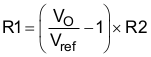
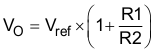
        1. 8.2.1.1 Programming the TPS71501-Q1 Adjustable LDO Regulator
        2. 8.2.1.2 External Capacitor Requirements
        3. 8.2.1.3 Input and Output Capacitor Requirements
        4. 8.2.1.4 Reverse Current
        5. 8.2.1.5 Feed-Forward Capacitor (CFF)
        6. 8.2.1.6 Power Dissipation (PD)
        7. 8.2.1.7 Estimating Junction Temperature
      2. 8.2.2 Application Curves
    3. 8.3 Power Supply Recommendations
    4. 8.4 Layout
      1. 8.4.1 Layout Guidelines
        1. 8.4.1.1 Power Dissipation
      2. 8.4.2 Layout Example
  10. Device and Documentation Support
    1. 9.1 Device Support
      1. 9.1.1 Development Support
        1. 9.1.1.1 Evaluation Module
        2. 9.1.1.2 Spice Models
      2. 9.1.2 Device Nomenclature
    2. 9.2 Documentation Support
      1. 9.2.1 Related Documentation
    3. 9.3 ドキュメントの更新通知を受け取る方法
    4. 9.4 サポート・リソース
    5. 9.5 Trademarks
    6. 9.6 静電気放電に関する注意事項
    7. 9.7 用語集
  11. 10Mechanical, Packaging, and Orderable Information

パッケージ・オプション

デバイスごとのパッケージ図は、PDF版データシートをご参照ください。

メカニカル・データ(パッケージ|ピン)
  • DCK|5
サーマルパッド・メカニカル・データ
発注情報

Programming the TPS71501-Q1 Adjustable LDO Regulator

The output voltage of the TPS71501-Q1 adjustable regulator is programmed using an external resistor divider as shown in Figure 8-3. The output voltage is calculated using Equation 2.

Equation 2. GUID-A2B9C678-DD47-4021-BBF7-3C160174A025-low.gif

where:

  • VREF = 1.205 V typ (the internal reference voltage)
GUID-20230324-SS0I-WKWN-QDZH-M83GJKTKLG1B-low.svg Figure 8-3 TPS71501-Q1 Adjustable LDO Regulator Programming

Choose resistors R1 and R2 for an approximately 1.5-μA divider current. Lower value resistors can be used for improved noise performance, but the solution consumes more power. Avoid higher resistor values because leakage current into and out of FB across R1 and R2 creates an offset voltage that artificially increases or decreases the feedback voltage and thus erroneously decreases or increases VO. The recommended design procedure is to choose R2 equal to 1 MΩ to set the divider current at 1.5 μA and then calculate R1 using Equation 3.

Equation 3. GUID-E8A42FFE-3BB4-489C-8849-AF4BBA02FC2C-low.gif