SLVSBM4C September 2012 – January 2016 TPS717-Q1
PRODUCTION DATA.
- 1 Features
- 2 Applications
- 3 Description
- 4 Revision History
- 5 Pin Configuration and Functions
- 6 Specifications
- 7 Detailed Description
- 8 Application and Implementation
- 9 Power Supply Recommendations
- 10Layout
- 11Device and Documentation Support
- 12Mechanical, Packaging, and Orderable Information
パッケージ・オプション
メカニカル・データ(パッケージ|ピン)
サーマルパッド・メカニカル・データ
- DRV|6
発注情報
8 Application and Implementation
NOTE
Information in the following applications sections is not part of the TI component specification, and TI does not warrant its accuracy or completeness. TI’s customers are responsible for determining suitability of components for their purposes. Customers should validate and test their design implementation to confirm system functionality.
8.1 Application Information
The TPS717-Q1 belongs to a family of new generation LDO regulators that use innovative circuitry to achieve ultra-wide bandwidth and high loop gain, resulting in extremely high PSRR at very low headroom (VIN – VOUT). Fixed voltage versions provide a noise reduction pin to bypass noise generated by the band-gap reference and to improve PSRR when a quick-start circuit fast-charges this capacitor. These features, combined with low noise, enable, low ground pin current, and ultra-small packaging, make this part ideal for automotive applications. This family of regulators offers sub-band-gap output voltages, current limit, and thermal protection, and is fully specified from –40°C to 125°C.
8.1.1 Transient Response
As with any regulator, increasing the size of the output capacitor reduces overshoot or undershoot magnitude but increases duration of the transient. The TPS717-Q1 has an ultra-wide loop bandwidth that allows it to respond quickly to load transient events. As with any regulator, the loop bandwidth is finite and the initial transient voltage peak is controlled by the sizing of the output capacitor. Typically, larger output capacitors reduce the peak and also reduce the bandwidth of the LDO, thus slowing the response time.
8.1.2 Input and Output Capacitor Requirements
Although an input capacitor is not required for stability, good analog design practice is to connect a 0.1-μF or larger low equivalent series resistance (ESR) capacitor from IN to GND near the regulator. This capacitor counteracts reactive input sources and improves transient response, noise rejection, and ripple rejection. A higher-value capacitor may be necessary if large, fast rise-time load transients are anticipated or if the device is located several inches from the power source. If source impedance is not sufficiently low, a 0.1-μF input capacitor may be necessary to ensure stability.
The TPS717-Q1 is designed to be stable with ceramic output capacitors of values 1 μF or larger. The X5R- and X7R-type capacitors are best because they have minimal variation in value and ESR over temperature. The maximum ESR of the output capacitor must be less than 1 Ω. The minimum output capacitance is increased to 5 μF or larger if using an R2 value outside of the range of 160 kΩ to 320 kΩ.
8.1.3 Dropout Voltage
The TPS717-Q1 uses a PMOS pass transistor to achieve low dropout. When (VIN – VOUT) is less than the dropout voltage (VDO), the PMOS pass device is in its linear region of operation and the input-to-output resistance is the RDSon of the PMOS pass element. VDO scales approximately with output current because the PMOS device functions as a resistor in dropout.
As with any linear regulator, PSRR and transient response are degraded when (VIN – VOUT) approaches dropout. This effect is illustrated in Figure 15 through Figure 17 in the Typical Characteristics section.
8.1.4 Power Dissipation
The ability to remove heat from the die is different for each package type, presenting different considerations in the printed circuit board (PCB) layout. The PCB area around the device that is free of other components moves the heat from the device to the ambient air. Performance data for JEDEC low- and high-K boards are given in the Thermal Information table. Using heavier copper increases the effectiveness in removing heat from the device. The addition of plated through-holes to heat-dissipating layers also improves the heatsink effectiveness.
Power dissipation depends on input voltage and load conditions. Power dissipation (PD) is equal to the product of the output current times the voltage drop across the output pass element (VIN to VOUT), as shown in Equation 2:

8.1.5 Output Noise
In most LDOs, the band gap is the dominant noise source. If a noise reduction capacitor (CNR) is used with the TPS717-Q1, the band gap does not contribute significantly to noise. Instead, noise is dominated by the output resistor divider and the error amplifier input. To minimize noise in a given application, use a 0.01-μF (minimum) noise reduction capacitor; for the adjustable version, smaller value resistors in the output resistor divider reduce noise. A parallel combination that gives 2.5 μA of divider current has the same noise performance as a fixed voltage version.
Equation 3 approximates the total noise referred to the feedback point (FB pin) when CNR = 0.01 μF:

8.2 Typical Application
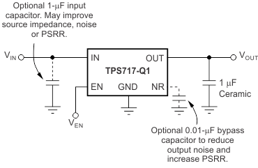
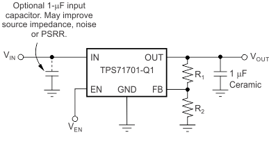
Figure 33 shows the basic circuit connections for the fixed voltage options. Figure 34 gives the connections for the adjustable output version (TPS71701-Q1). Note that the NR pin is not available on the adjustable version.
 Figure 33. Typical Application Circuit
 (Fixed Voltage Versions)
 Figure 34. Typical Application Circuit
 (Adjustable Voltage Version)
8.2.1 Design Requirements
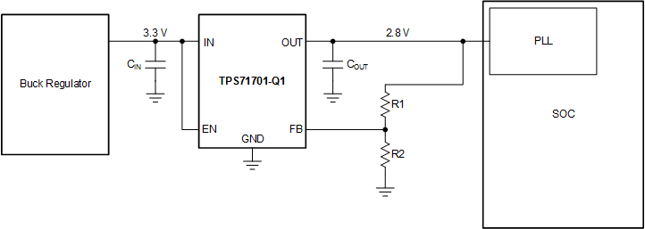
Table 2 summarizes the design requirements for Figure 35.
Table 2. Design Requirements
| PARAMETER | DESIGN REQUIREMENT |
|---|---|
| Input voltage | 3.3 V, ±10% |
| Output voltage | 2.8 V, ±5% |
| Output current | 100 mA typical, 150 mA peak |
| Output voltage transient deviation | 5% |
| Maximum ambient temperature | 85°C |
8.2.2 Detailed Design Procedure
8.2.2.1 Design Considerations
For the adjustable version (TPS71701-Q1), the NR pin is replaced with a feedback (FB) pin. The voltage on this pin sets the output voltage and is determined by the values of R1 and R2. The values of R1 and R2 can be calculated for any voltage using the formula given in Equation 4:
The value of R2 directly affects the operation of the device and must be chosen in the range of approximately
160 kΩ to 332 kΩ. Sample resistor values for common output voltages are shown in Table 3.
Table 3. Sample 1% Resistor Values For Common Output Voltages
| VOUT | R1 | R2 |
|---|---|---|
| 1 | 80.6 kΩ | 324 kΩ |
| 1.2 | 162 kΩ | 324 kΩ |
| 1.5 | 294 kΩ | 332 kΩ |
| 1.8 | 402 kΩ | 324 kΩ |
| 2.5 | 665 kΩ | 316 kΩ |
| 3.3 | 1.02 MΩ | 324 kΩ |
| 5 | 1.74 MΩ | 332 kΩ |
8.2.2.2 Powering a PLL Integrated on an SOC
Figure 35 shows the TPS71701-Q1 powering a phase-locked loop (PLL) that is integrated into a system-on-a-chip (SOC).
 Figure 35. Typical Application Circuit: PLL on an SOC
8.2.2.3 Design Considerations
Use the input and output capacitors to ensure the voltage transient requirements. A 1-µF input and 1-µF output capacitor are selected to maximize the capacitance and minimize capacitor size.
R2 is chosen to be 158 kΩ for optimal noise and PSRR, and by Equation 2, R1 is selected to be 402 kΩ. Both R1 and R2 must be 1% tolerance resistors to meet the dc accuracy specification over line, load, and temperature.
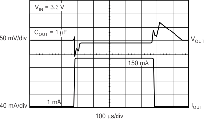
8.2.3 Application Curve
 Figure 36. Load Transient Response
8.3 Do's and Don'ts
Do place at least one 1-µF ceramic capacitor as close as possible to both the input and output pins of the LDO.
Do not place the output capacitor more than 10 mm away from the regulator.
Do not place any components in the feedback loop except for the input, output, and feed-forward capacitor and the feedback resistors.
Do not exceed the device absolute maximum ratings.
Do not float the enable (EN) pin.
