SLVSBM4C September 2012 – January 2016 TPS717-Q1
PRODUCTION DATA.
- 1 Features
- 2 Applications
- 3 Description
- 4 Revision History
- 5 Pin Configuration and Functions
- 6 Specifications
- 7 Detailed Description
- 8 Application and Implementation
- 9 Power Supply Recommendations
- 10Layout
- 11Device and Documentation Support
- 12Mechanical, Packaging, and Orderable Information
パッケージ・オプション
メカニカル・データ(パッケージ|ピン)
サーマルパッド・メカニカル・データ
- DRV|6
発注情報
6 Specifications
6.1 Absolute Maximum Ratings
over operating temperature range (unless otherwise noted), all voltages are with respect to GND(1)| MIN | MAX | UNIT | ||
|---|---|---|---|---|
| Voltage | VIN | –0.3 | 7 | V |
| VFB | –0.3 | 3.6 | ||
| VNR | –0.3 | 3.6 | ||
| VEN | –0.3 | VIN + 0.3 V(2) | ||
| VOUT | –0.3 | 7 | ||
| Current | IOUT | Internally limited | A | |
| Continuous total power dissipation | PDISS | See Thermal Information table | ||
| Ambient temperature | TA | –40 | 125 | °C |
| Operating junction temperature | TJ | –55 | 150 | °C |
| Storage temperature | Tstg | –55 | 150 | °C |
(1) Stresses beyond those listed under Absolute Maximum Ratings may cause permanent damage to the device. These are stress ratings only, which do not imply functional operation of the device at these or any other conditions beyond those indicated under Recommended Operating Conditions. Exposure to absolute-maximum-rated conditions for extended periods may affect device reliability.
(2) VEN absolute maximum rating is VIN + 0.3 V or 7 V, whichever is greater.
6.2 ESD Ratings
| VALUE | UNIT | ||||
|---|---|---|---|---|---|
| V(ESD) | Electrostatic discharge | Human body model (HBM), per AEC Q100-002(1) | ±2000 | V | |
| TPS717-Q1 in DCK and DSE packages | |||||
| V(ESD) | Electrostatic discharge | Charged device model (CDM), per AEC Q100-011 | All pins | ±750 | V |
| Corner pins, DCK (1, 3, 4, and 5) |
±750 | ||||
| Corner pins, DSE (1, 3, 4, and 6) |
±750 | ||||
| TPS717-Q1 in DRV package | |||||
| V(ESD) | Electrostatic discharge | Charged device model (CDM), per AEC Q100-011 | All pins | ±500 | V |
| Corner pins (1, 3, 4, and 6) | ±750 | ||||
(1) AEC Q100-002 indicates HBM stressing is done in accordance with the ANSI/ESDA/JEDEC JS-001 specification.
6.3 Recommended Operating Conditions
over operating free-air temperature range (unless otherwise noted)| MIN | NOM | MAX | UNIT | ||
|---|---|---|---|---|---|
| VIN | Input voltage | 2.5 | 6.5 | V | |
| VOUT | Output voltage | 0.9 | 5 | V | |
| IOUT | Output current | 0 | 150 | mA | |
| VEN | Enable voltage | 0 | VIN | V | |
| CIN | Input capacitor | 1 | µF | ||
| R2 | Lower feedback resistor | 160 | 320 | 332 | kΩ |
| CNR | Noise reduction capacitor | 10 | nF | ||
| COUT | Output capacitor | 1(1) | 100 | µF | |
| TJ | Junction temperature | –40 | 125 | °C | |
(1) Adjustable voltage version only. When using feedback resistors that are smaller than recommended, the minimum output capacitance must be greater than 5 µF.
6.4 Thermal Information
| THERMAL METRIC(1) | TPS717-Q1 | UNIT | |||
|---|---|---|---|---|---|
| DCK (SOT) | DRV (WSON) | DSE (WSON) | |||
| 5 PINS | 6 PINS | 6 PINS | |||
| RθJA | Junction-to-ambient thermal resistance | 279.2 | 71.1 | 190.5 | °C/W |
| RθJC(top) | Junction-to-case (top) thermal resistance | 57.5 | 96.5 | 94.9 | °C/W |
| RθJB | Junction-to-board thermal resistance | 74.1 | 40.5 | 149.3 | °C/W |
| ψJT | Junction-to-top characterization parameter | 0.8 | 2.7 | 6.4 | °C/W |
| ψJB | Junction-to-board characterization parameter | 73.1 | 40.9 | 152.8 | °C/W |
| RθJC(bot) | Junction-to-case (bottom) thermal resistance | n/a | 10.7 | n/a | °C/W |
(1) For more information about traditional and new thermal metrics, see the IC Package Thermal Metrics application report, SPRA953.
6.5 Electrical Characteristics
Over operating temperature range (TJ, TA = –40°C to 125°C), VIN = VOUT(nom) + 0.5 V or 2.5 V, whichever is greater; IOUT = 0.5 mA, VEN = VIN, COUT = 1 μF, CNR = 0.01 μF, unless otherwise noted. For the adjustable version (TPS71701-Q1), VOUT = 2.8 V. Typical values are at TA = 25°C.| PARAMETER | TEST CONDITIONS | MIN | TYP | MAX | UNIT | |||
|---|---|---|---|---|---|---|---|---|
| VIN | Input voltage range(1) | 2.5 | 6.5 | V | ||||
| VFB | Feedback pin voltage (TPS71701) | IOUT = 5 mA | –2% | 0.793 | 2% | V | ||
| VOUT | Output voltage range | TPS717-Q1 | 0.9 | 5 | V | |||
| TPS71701-Q1 | 0.9 | 6.5 – VDO | ||||||
| VOUT | Output accuracy (nominal) | TA = 25°C | ±2.5 | mV | ||||
| Output accuracy (VOUT < 1 V) |
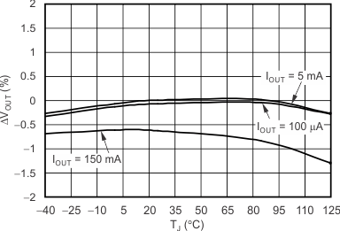
Over VIN, IOUT, temperature(3) | VOUT + 0.5 V ≤ VIN ≤ 6.5 V, 0 mA ≤ IOUT ≤ 150 mA |
–30 | 30 | ||||
| Output accuracy (VOUT ≥ 1 V) |
Over VIN, IOUT, temperature(3) | VOUT + 0.5 V ≤ VIN ≤ 6.5 V, 0 mA ≤ IOUT ≤ 150 mA |
–3% | 3% | ||||
| ΔVOUT(ΔVIN) | Line regulation(1) | VOUT(nom) + 0.5 V ≤ VIN ≤ 6.5 V, IOUT = 5 mA |
125 | μV/V | ||||
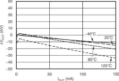
| ΔVOUT(ΔIOUT) | Load regulation | 0 mA ≤ IOUT ≤ 150 mA | 70 | μV/mA | ||||
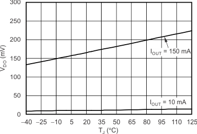
| VDO | Dropout voltage(2)
(VIN = VOUT(nom) – 0.1 V) |
IOUT = 150 mA | 170 | 300 | mV | |||
| ILIM (fixed) | Output current limit (fixed output) | VOUT = 0.9 × VOUT(nom) | 200 | 325 | 575 | mA | ||
| ILIM (adjustable) | Output current limit (TPS71701-Q1) | VOUT = 0.9 × VOUT(nom) | 200 | 325 | 575 | mA | ||
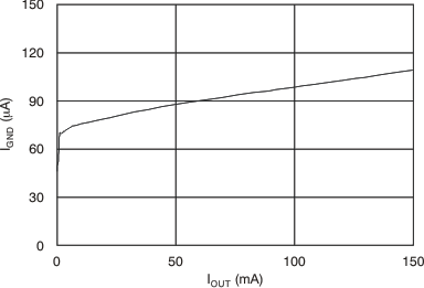
| IGND | Ground pin current | IOUT = 0.1 mA | 45 | 80 | μA | |||
| IOUT = 150 mA | 100 | |||||||
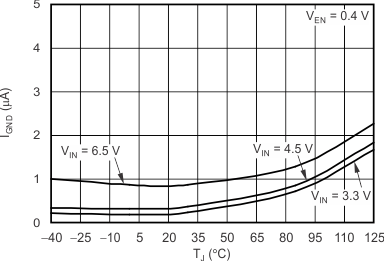
| ISHDN | Shutdown current (IGND) | VEN ≤ 0.4 V, 2.5 V ≤ VIN < 4.5 V, TA = –40°C to 125°C |
0.20 | 1.5 | μA | |||
| VEN ≤ 0.4 V, 4.5 V ≤ VIN ≤ 6.5 V, TA = –40°C to 125°C |
0.90 | |||||||
| VEN ≤ 0.4 V, 2.5 V ≤ VIN < 4.5 V, TA = –40°C to 125°C, DRV package |
2 | |||||||
| IFB | Feedback pin current (TPS71701-Q1) | 0.02 | 1 | μA | ||||
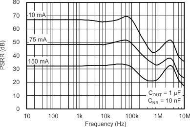
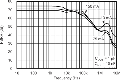
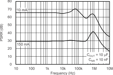
| PSRR | Power-supply rejection ratio | VIN = 3.8 V, VOUT = 2.8 V, IOUT = 150 mA |
f = 100 Hz | 70 | dB | |||
| f = 1 kHz | 70 | |||||||
| f = 10 kHz | 67 | |||||||
| f = 100 kHz | 67 | |||||||
| f = 1 MHz | 45 | |||||||
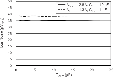
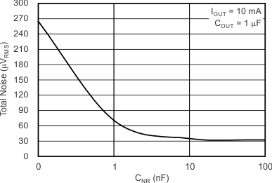
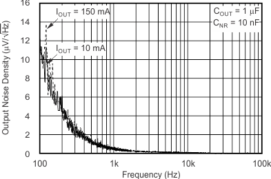
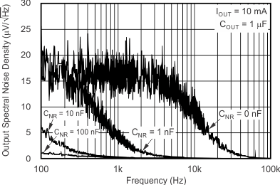
| Vn | Output noise voltage | BW = 100 Hz to 100 kHz, VIN = 3.8 V, VOUT = 2.8 V, IOUT = 10 mA |
CNR = none | 95 × VOUT | μVRMS/V | |||
| CNR = 0.001 μF | 25 × VOUT | |||||||
| CNR = 0.01 μF | 12.5 × VOUT | |||||||
| CNR = 0.1 μF | 11.5 × VOUT | |||||||
| tSTR | Startup time | VOUT = 90% VOUT(nom), RL = 19 Ω, COUT = 1 μF |
0.9 V ≤ VOUT ≤ 1.6 V, CNR = 0.001 μF | 0.700 | ms | |||
| 1.6 V < VOUT < VOUT(max), CNR = 0.01 μF | 0.160 | |||||||
| VEN(high) | Enable high (enabled) | VIN ≤ 5.5 V | 1.2 | 6.5(4) | V | |||
| 5.5 V < VIN ≤ 6.5 V | 1.25 | 6.5 | ||||||
| VEN(low) | Enable low (shutdown) | 0 | 0.4 | V | ||||
| IEN(high) | Enable pin current, enabled | EN = 6.5 V | 0.02 | 1 | μA | |||
| Tsd | Thermal shutdown temperature | Shutdown, temperature increasing | 160 | °C | ||||
| Reset, temperature decreasing | 140 | |||||||
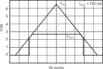
| UVLO | Undervoltage lockout | VIN rising | 2.45 | 2.49 | V | |||
| Hysteresis | VIN falling | 150 | mV | |||||
(1) Minimum VIN = VOUT + VDO or 2.5 V, whichever is greater.
(2) VDO is not measured for devices with VOUT(nom) < 2.6 V because minimum VIN = 2.5 V.
(3) Does not include external resistor tolerances.
(4) Maximum VEN(high) = VIN + 0.3 or 6.5 V, whichever is smaller.
6.6 Typical Characteristics
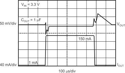
Over operating temperature range (TJ, TA = –40°C to 125°C), VIN = VOUT(nom) + 0.5 V or 2.5 V, whichever is greater; IOUT = 0.5 mA, VEN = VIN, COUT = 1 μF, CNR = 0.01 μF, unless otherwise noted. For the adjustable version (TPS71701-Q1), VOUT = 2.8 V. Typical values are at TA = 25°C.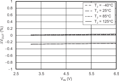
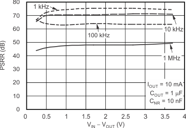
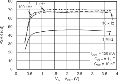
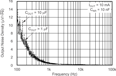
Output Capacitance
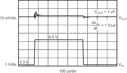
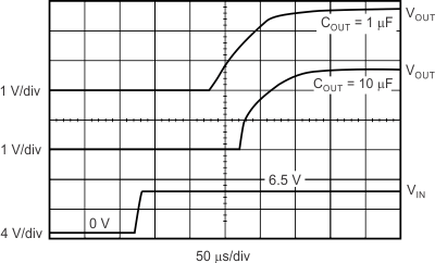
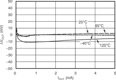
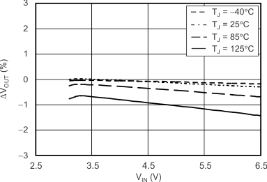
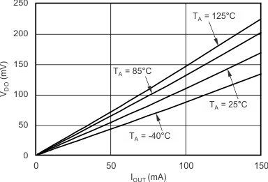
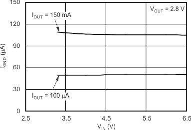
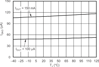
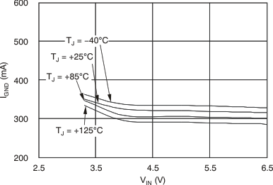
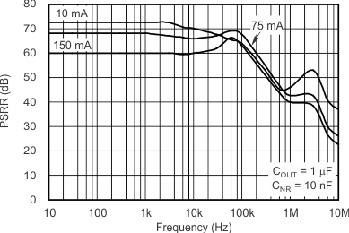
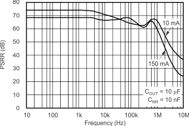
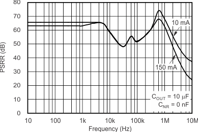
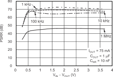
Output Current
Noise Reduction
