JAJSGW8B October 2014 – February 2019 TPS735-Q1
PRODUCTION DATA.
- 1 特長
- 2 アプリケーション
- 3 概要
- 4 改訂履歴
- 5 Pin Configuration and Functions
- 6 Specifications
- 7 Detailed Description
- 8 Application and Implementation
- 9 Power Supply Recommendations
- 10Layout
- 11デバイスおよびドキュメントのサポート
- 12メカニカル、パッケージ、および注文情報
パッケージ・オプション
デバイスごとのパッケージ図は、PDF版データシートをご参照ください。
メカニカル・データ(パッケージ|ピン)
- DRB|8
サーマルパッド・メカニカル・データ
発注情報
10.1.4 Power Dissipation
The ability to remove heat from the die is different for each package type, presenting different considerations in the PCB layout. The PCB area around the device that is free of other components moves the heat from the device to the ambient air. Performance data for JEDEC low- and high-K boards are given in the table. Using heavier copper increases the effectiveness in removing heat from the device. The addition of plated through-holes to heat-dissipating layers also improves the heatsink effectiveness.
Power dissipation depends on input voltage and load conditions. Power dissipation is equal to the product of the output current and the voltage drop across the output pass element, as shown in Equation 2.
NOTE
When the device is used in a condition of high input and low output voltages, PD can exceed the junction temperature rating even when the ambient temperature is at room temperature.
Equation 3 is an example calculation for the power dissipation (PD) of the DRB package.
Power dissipation can be minimized and greater efficiency can be achieved by using the lowest possible input voltage necessary to achieve the required output performance.
On the DRB package, the primary conduction path for heat is through the exposed thermal pad to the PCB. The pad can be connected to ground or left floating; however, the pad must be attached to an appropriate amount of copper PCB area to ensure the device does not overheat. The maximum allowable junction-to-ambient thermal resistance depends on the maximum ambient temperature, maximum device junction temperature, and power dissipation of the device. Use Equation 4 to calculate the maximum junction-to-ambient thermal resistance.

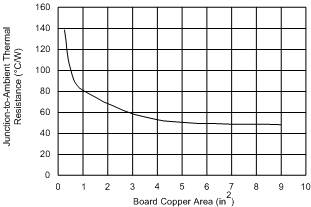
Knowing the maximum RθJA, the minimum amount of PCB copper area needed for appropriate heatsinking can be estimated using Figure 22.

NOTE:
The RθJA value at a board size of 9 in2 (that is, 3 in × 3 in) is a JEDEC standard.Figure 22 shows the variation of RθJA as a function of copper area in the board that is connected to the thermal pad. Figure 22 is intended only as a guideline to demonstrate the effects of heat spreading in the ground plane and is not to be used to calculate actual thermal performance.
NOTE
When the device is mounted on an application PCB, TI strongly recommends using ΨJT and ΨJB, as explained in the Estimating Junction Temperature section.